


2. (10 points) or the given FET network shown in the given figure etermine the following if kn'(W/L)=4 mA/V2 and Vt 2V: 1) VGs 2) Vs 3) VD 4) VDs 5) Verify the operation mode for transistor if it is working in saturation or triode and why? VDD 15 V 4mA NE=2V ヒn 0.5 mA Rp 10k o VD V +75V o -o Vs g=+7s Rs 10 k 7 MQ
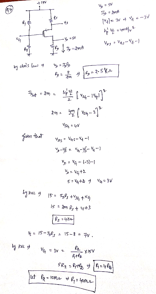
rerdrtre voltage D the ariode region: Operation Conditions Overdrive voltage: tor 20 nw e-V. Q4. (10 the circuit in the below figure (Find the values of RD, s operates 1V from the edge of saturation: VDs 4mA/V2. Make sure the values of Ri and R2 in the range of Mega Ohm. R2), so that the transistor 3V and k'pW/L= VGS-V-1 +15 V VDs=Vas-Ne-1 R Rs VD= o Vs VGO ID=2mA o Vp=SN R2 Rp KPWAMA
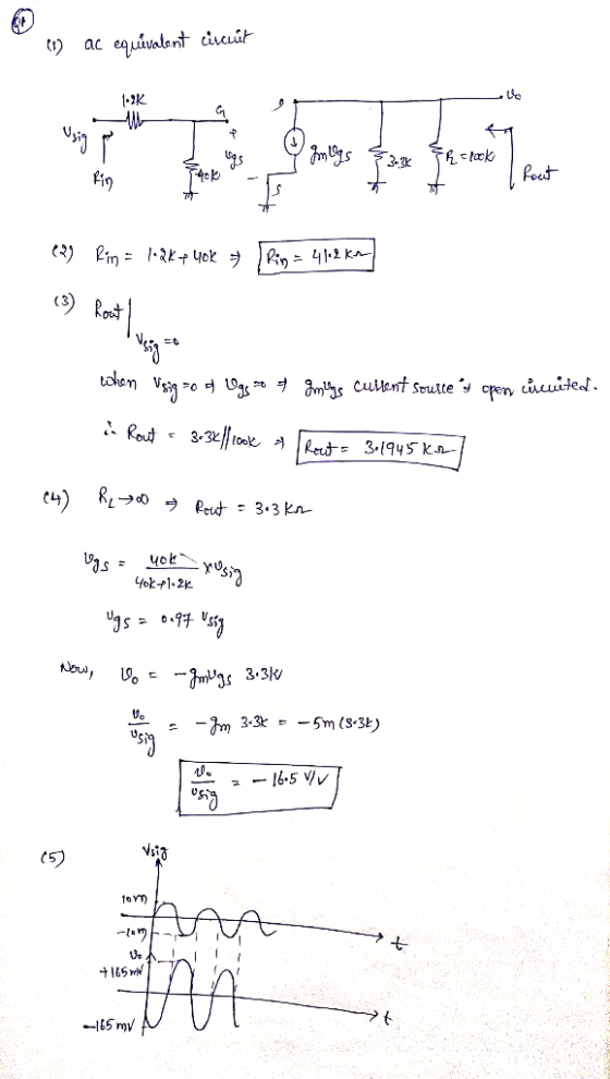
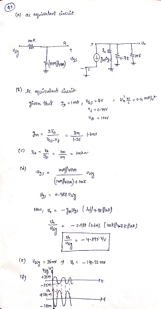
Ove tar Operation in the triode region: Conditions: V Overdrive voltage Vow ee-V. Q3. (10 points) the small AC equivalent circuit for the network shown below. b) Find c) Determine ro- d) Determine Gv Vo/ Vsig- e) Determine the output voltage (Vo) for the network shown below if 35mV, ID= 1mA, Vas=2V, kn' (W/L) = 0.4 mA/V2, V 0.75V and VA1 put with Vsig f) Sketch the waveform of the output voltage (Vo). a sine wave G=O 4.7 kn 47 MQ o V 100 kn 0.1 F 10kn 0.01 F 10 F 10 Mn2kN
Homework Answers

Add Answer to:
V.+w Operation in the triode reglon Condition v. e Wov 20 Vos uov os os-V (2) p V, so onl+Pala Characteristics Same rel...
will the answer be the same if it was in enhacement mode?? please explain first image...
 will the answer be the same if it was in enhacement mode??
please explain
first image is QUESTION
second image is ANSWER
just answer and explain my QUESTION i asked..
The gate-to-source voltage of the depletion-mode, n-channel MOSFET shown in the circuit below is 1 V. The various operating regions of the MOSFET are described below: Cutoff Region: (VGS<V) b=0 Triode Region: (VGs > V, and ved >V) id=K [2 (Vgs - Vp) Vps - Vps?1 Saturation Region: (VGs >...
will the answer be the same if it was in enhacement mode??
please explain
first image is QUESTION
second image is ANSWER
just answer and explain my QUESTION i asked..
The gate-to-source voltage of the depletion-mode, n-channel MOSFET shown in the circuit below is 1 V. The various operating regions of the MOSFET are described below: Cutoff Region: (VGS<V) b=0 Triode Region: (VGs > V, and ved >V) id=K [2 (Vgs - Vp) Vps - Vps?1 Saturation Region: (VGs >...
2. (25) You have been given an N-channel enhancement mode MOSFET to be used in the...
 2. (25) You have been given an N-channel enhancement mode MOSFET to be used in the next circuits. The NMOS has the characteristics of Ky = 1.0 mA/V,20, and Vin =1.0 V. A graph o current-voltage characteristics is shown on the next page of the test. (a) Determine resistor values (R. R. Ro Rs) so that Ipo = 4 mA and lose Let Ri= R/ || R 100 K and Vas Vs. Vpp = 12 V. VID = ID. RD"...
#4 The accompanying circuit shows a 4-resistor biased JFET transistor Determine the values of Rp and Rs so that the Q-point is equal to, VDsq 10 V and IDg 5 mA . For the JFET take IDss = 10 mA...
 #4
The accompanying circuit shows a 4-resistor biased JFET transistor Determine the values of Rp and Rs so that the Q-point is equal to, VDsq 10 V and IDg 5 mA . For the JFET take IDss = 10 mA, VP =-5 V and λ 0 . The circuit parameters are, R1-740 k, R2-22 1.85 ka, Rs-85 ㏀ and RL-3.5 ㏀. Take the power supply VDD 24 V 2- Vo R1 Vi R2 Signal generator 4-In reference to the circuit...
#4
The accompanying circuit shows a 4-resistor biased JFET transistor Determine the values of Rp and Rs so that the Q-point is equal to, VDsq 10 V and IDg 5 mA . For the JFET take IDss = 10 mA, VP =-5 V and λ 0 . The circuit parameters are, R1-740 k, R2-22 1.85 ka, Rs-85 ㏀ and RL-3.5 ㏀. Take the power supply VDD 24 V 2- Vo R1 Vi R2 Signal generator 4-In reference to the circuit...
Please answer clearly Question 2 The amplifier shown in Figure 2 has the following parameters: Kn(W/L)-1 mA/V2, V-1 V Determine a) Voltage gain (Vo/vi) b) Input resistance (R) c) Output resistance (R...
 Please answer clearly
Question 2 The amplifier shown in Figure 2 has the following parameters: Kn(W/L)-1 mA/V2, V-1 V Determine a) Voltage gain (Vo/vi) b) Input resistance (R) c) Output resistance (Ro) d) Maximum output voltage swing so as the amplifier stays in saturation mode. Assume VDD-20 V, R1-2.5 ΚΩ, R2-1KQ, R3-0.5 ΚΩ, R4-5 MQ, R5_1ΜΩ. R4 R1 R5 R2 Ro R3
Question 2 The amplifier shown in Figure 2 has the following parameters: Kn(W/L)-1 mA/V2, V-1 V Determine a)...
Please answer clearly
Question 2 The amplifier shown in Figure 2 has the following parameters: Kn(W/L)-1 mA/V2, V-1 V Determine a) Voltage gain (Vo/vi) b) Input resistance (R) c) Output resistance (Ro) d) Maximum output voltage swing so as the amplifier stays in saturation mode. Assume VDD-20 V, R1-2.5 ΚΩ, R2-1KQ, R3-0.5 ΚΩ, R4-5 MQ, R5_1ΜΩ. R4 R1 R5 R2 Ro R3
Question 2 The amplifier shown in Figure 2 has the following parameters: Kn(W/L)-1 mA/V2, V-1 V Determine a)...
+20 V ID- 6 mA RG Figure 7-3 21) Refer to Figure 7-3. In this circuit,...
 +20 V ID- 6 mA RG Figure 7-3 21) Refer to Figure 7-3. In this circuit, VGs is biased correctly for proper operation. This means 21) that VGS is negative. C) either negative or positive. D) positive. 22) Refer to Figure 7-3. Calculate the value of VDs 22) A) 0 V B)-2 V C) 2V D) 4V o-vs Vos + 20 V Cs キDj R1 Figure 9-3 23) Refer to Figure 9-3. The de voltage across RL was measured at...
Problem 3: Design Problem On Figure P3a, you have a Common Source (CS) n-channel MOSFET amplifier....
 Problem 3: Design Problem On Figure P3a, you have a Common Source (CS) n-channel MOSFET amplifier. Notice the absence of a source resistor Rsig and load resistor R. If we know how the present amplifier (the one on Figure P3a) behaves without Rsig and RL, we can infer its behaviors if Rsig and R were to be added. design the amplifier circuit on Figure P3a, i.e., you have to find appropriate values for RGj You are to RG,, RD, and...
Question 2: a) Find the value of Vgs? b) If the threshold voltage of the NMOS 0.7V, identify the region o...
 Question 2: a) Find the value of Vgs? b) If the threshold voltage of the NMOS 0.7V, identify the region of operation for the MOSFET (i.e. Triode Saturation or Cutoff) v,= 10V SATE e) Write the formula to calculate Current (ID) for the circuit in Figure 1 Fig. 1 Question 3: a) Find the value of Vgs* b) If the threshold voltage of the NMOS 0.7V, identify the region of operation for the MOSFET (i.e. Triode, Saturation or Cutoff) c)...
 will the answer be the same if it was in enhacement mode??
please explain
first image is QUESTION
second image is ANSWER
just answer and explain my QUESTION i asked..
The gate-to-source voltage of the depletion-mode, n-channel MOSFET shown in the circuit below is 1 V. The various operating regions of the MOSFET are described below: Cutoff Region: (VGS<V) b=0 Triode Region: (VGs > V, and ved >V) id=K [2 (Vgs - Vp) Vps - Vps?1 Saturation Region: (VGs >...
will the answer be the same if it was in enhacement mode??
please explain
first image is QUESTION
second image is ANSWER
just answer and explain my QUESTION i asked..
The gate-to-source voltage of the depletion-mode, n-channel MOSFET shown in the circuit below is 1 V. The various operating regions of the MOSFET are described below: Cutoff Region: (VGS<V) b=0 Triode Region: (VGs > V, and ved >V) id=K [2 (Vgs - Vp) Vps - Vps?1 Saturation Region: (VGs >...
 2. (25) You have been given an N-channel enhancement mode MOSFET to be used in the next circuits. The NMOS has the characteristics of Ky = 1.0 mA/V,20, and Vin =1.0 V. A graph o current-voltage characteristics is shown on the next page of the test. (a) Determine resistor values (R. R. Ro Rs) so that Ipo = 4 mA and lose Let Ri= R/ || R 100 K and Vas Vs. Vpp = 12 V. VID = ID. RD"...
 #4
The accompanying circuit shows a 4-resistor biased JFET transistor Determine the values of Rp and Rs so that the Q-point is equal to, VDsq 10 V and IDg 5 mA . For the JFET take IDss = 10 mA, VP =-5 V and λ 0 . The circuit parameters are, R1-740 k, R2-22 1.85 ka, Rs-85 ㏀ and RL-3.5 ㏀. Take the power supply VDD 24 V 2- Vo R1 Vi R2 Signal generator 4-In reference to the circuit...
#4
The accompanying circuit shows a 4-resistor biased JFET transistor Determine the values of Rp and Rs so that the Q-point is equal to, VDsq 10 V and IDg 5 mA . For the JFET take IDss = 10 mA, VP =-5 V and λ 0 . The circuit parameters are, R1-740 k, R2-22 1.85 ka, Rs-85 ㏀ and RL-3.5 ㏀. Take the power supply VDD 24 V 2- Vo R1 Vi R2 Signal generator 4-In reference to the circuit...
 Please answer clearly
Question 2 The amplifier shown in Figure 2 has the following parameters: Kn(W/L)-1 mA/V2, V-1 V Determine a) Voltage gain (Vo/vi) b) Input resistance (R) c) Output resistance (Ro) d) Maximum output voltage swing so as the amplifier stays in saturation mode. Assume VDD-20 V, R1-2.5 ΚΩ, R2-1KQ, R3-0.5 ΚΩ, R4-5 MQ, R5_1ΜΩ. R4 R1 R5 R2 Ro R3
Question 2 The amplifier shown in Figure 2 has the following parameters: Kn(W/L)-1 mA/V2, V-1 V Determine a)...
Please answer clearly
Question 2 The amplifier shown in Figure 2 has the following parameters: Kn(W/L)-1 mA/V2, V-1 V Determine a) Voltage gain (Vo/vi) b) Input resistance (R) c) Output resistance (Ro) d) Maximum output voltage swing so as the amplifier stays in saturation mode. Assume VDD-20 V, R1-2.5 ΚΩ, R2-1KQ, R3-0.5 ΚΩ, R4-5 MQ, R5_1ΜΩ. R4 R1 R5 R2 Ro R3
Question 2 The amplifier shown in Figure 2 has the following parameters: Kn(W/L)-1 mA/V2, V-1 V Determine a)...
 +20 V ID- 6 mA RG Figure 7-3 21) Refer to Figure 7-3. In this circuit, VGs is biased correctly for proper operation. This means 21) that VGS is negative. C) either negative or positive. D) positive. 22) Refer to Figure 7-3. Calculate the value of VDs 22) A) 0 V B)-2 V C) 2V D) 4V o-vs Vos + 20 V Cs キDj R1 Figure 9-3 23) Refer to Figure 9-3. The de voltage across RL was measured at...
 Problem 3: Design Problem On Figure P3a, you have a Common Source (CS) n-channel MOSFET amplifier. Notice the absence of a source resistor Rsig and load resistor R. If we know how the present amplifier (the one on Figure P3a) behaves without Rsig and RL, we can infer its behaviors if Rsig and R were to be added. design the amplifier circuit on Figure P3a, i.e., you have to find appropriate values for RGj You are to RG,, RD, and...
 Question 2: a) Find the value of Vgs? b) If the threshold voltage of the NMOS 0.7V, identify the region of operation for the MOSFET (i.e. Triode Saturation or Cutoff) v,= 10V SATE e) Write the formula to calculate Current (ID) for the circuit in Figure 1 Fig. 1 Question 3: a) Find the value of Vgs* b) If the threshold voltage of the NMOS 0.7V, identify the region of operation for the MOSFET (i.e. Triode, Saturation or Cutoff) c)...
Most questions answered within 3 hours.
-
Suppose you have three events - X, Y, and Z - where X and Y are...
asked 19 minutes ago -
Consider the following bond: Face value = $1000; coupon rate =
8%; yield to maturity =...
asked 1 minute ago -
1.Discuss two reasons why some antibiotics show greater evidence
of bacterial resistance than others.
2.It is...
asked 4 minutes ago -
For a particular isomer of C8H18, the combustion reaction
produces 5099.5 kJ of heat per mole...
asked 29 minutes ago -
SETUP: MARKETING MANAGEMENT PLAN PURPOSE (VERSION #4)
DESCRIBE WHO YOUR MARKETING MANAGEMENT PLAN IS FOR, AND...
asked 16 minutes ago -
REPUBLICANS ARGUE THAT LABOR DEMAND IS ____, SO ____ JOBS WILL
BE LOST WHEN THE MINIMUM...
asked 26 minutes ago -
Predict the impact of high unemployment on the number and nature
of entrepreneurial startups. Speculate whether...
asked 37 minutes ago -
Suppose there is a duopoly of two identical firms, A and B,
facing a market inverse...
asked 50 minutes ago -
A camera with a lens diameter D = 3 mm and a focal length of f...
asked 58 minutes ago -
8. A drug company has a monopoly on a new class of
corticosteroid. The market demand...
asked 1 hour ago -
Is dividing a government a good or bad thing? How can this
problem be fixed? What...
asked 1 hour ago -
You need to implement a queue based on the doubly linked list.
(In C++) **PLEASE follow...
asked 1 hour ago