


Fig. 2 Question 4: a) Find the value of Vs ML b)If the threshold voltage of the NMOS 0.7V, identify the region of operation for the MOSFET (i.e. Triode Saturation or Cutoff) e) Write the formula to calculate Current (ID) for the circuit in Figure 3. Fig.3 Question 5: V5V a) Find the value of Vos* b) Find the value of V e) If the threshold voltage of the NMOS 0.7V, identify the region of operation for the MOSFET (i.e. Triode, Saturation or Cutoff) d Write the formula to calculate Current (I) for GS sad DS the circuit in Figure 4. Fig. 4 Question 6 a) What is channel length modulation? b) Draw the large signal model of a MOSFET when channel length modulation 0 e Draw the large signal model of a MOSFET when channel length modulation 10 Question 7: A 0.18-um fabrication process is specified to have t= 4 nm, ,450 cm/V-s, and V, 0.5 V Find the value of the process transconductance parameter k. For a MOSFET with minimum length fabricated in this process, find the required value of W so that the device exhibits a channel resistance F of I k2 at vasIV
Lecture Summary We discussed MOSFET biasing and different regions of operations. We further discussed IV characteristics of ideal and non-ideal MOSFET . Channel length modulation and effect of channel length modulation on current ID was also discussed during the lectures.
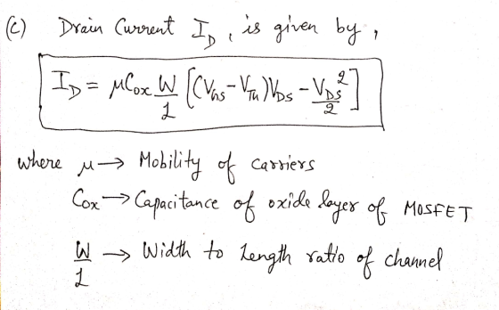
Question 2 a) Find the value of Vgs? b) If the threshold voltage of the NMOS = 0.7V, identify the region of operation for the MOSFET (i.e. Triode, Saturation or Cutoff) e) Write the formula to calculate Current (ID) for the circuit in Figure 1 R2 100 C BAT2 81 100 0 Fig. Question 3 VD a) Find the value of Vgs b) If the threshold voltage of the NMOS 0.7V, identify the region of operation for the MOSFET (i.e Triode, Saturation or Cutoff) e) Write the formula to calculate Current (ID) for the circuit in Figure 2 10V NMOS G BAT2 R1 100
Question 4: a) Find the value of Vos b) If the threshold voltage of the NMOS 0.7V, identify the region of operation for the MOSFET (i.e. Triode, Saturation or Cutoff) e) Write the formula to calculate Current (ID) for the circuit in Figure 3. Fig. 3 Question 5: 5V a)Find the value of VGs bFind the value of Vps e)If the threshold voltage of the NMOS 0.7V, identify the region of operation for the MOSFET (i.e. Triode, Saturation or Cutoff) d) Write the formula to calculate Current (I,) for the circuit in Figure 4 v ov Fig. 4 Question 6 a) What is channel length modulation? b) Draw the large signal model of a MOSFET when channel length modulation = 0. c) Draw the large signal model of a MOSFET when channel length modulation 1 0 Question 7: A 0.18-jum fabrication process is specified to have =4 nm, ,= 450 cm N-s, and V,= 05 V Find the value of the process transconductance parameterk. For a MOSFET with minimum length fabricated in this process, find the required value of W so that the device exhibits a channel resistance os of 1 k2 at v IV
Homework Answers


 As
per the HomeworkLib policy I needed to solve first question completely
but I have solved 2 questions for you, as you have posted multiple
questions.Feel free to ask if you have any query.Thank you.
As
per the HomeworkLib policy I needed to solve first question completely
but I have solved 2 questions for you, as you have posted multiple
questions.Feel free to ask if you have any query.Thank you.
Add Answer to:
Question 2: a) Find the value of Vgs? b) If the threshold voltage of the NMOS 0.7V, identify the region o...
Lecture Summary We discussed MOSFET biasing and different regions of operations. We further discussed IV character...
 Lecture Summary We discussed MOSFET biasing and different regions of operations. We further discussed IV characteristicss of ideal and non-ideal MOSFETS. Channel length modulation and effect of channel length modulation on current ID was also discussed during the lectures. Quentinductor and PN junction is also introduced in the lectures. Draw IV characteristics of an ideal diode. b Draw IV characteristics of a non-ideal diode with Vt 0.4V e Draw IV characteristics of an ideal MOSFET al d) Draw IV characteristics...
Vs 82 BATZ IOS = eration rrent (ID) for Fig. 3 VD 5V NMOS 10 0 BAT2 R1 1000 IOS . Triode, rrent (In) for Fig...
 Vs 82 BATZ IOS = eration rrent (ID) for Fig. 3 VD 5V NMOS 10 0 BAT2 R1 1000 IOS . Triode, rrent (In) for Fig. 4 Question 4: W a Find the value of Vas b If the threshold voltage of the NMOS = 0.7V, identify the region of operation for the MOSFET (i.e. Triode Saturation or Cutoff) e Write the formula to calculate Current (ID) for the circuit in Figure 3. Fig. 3 Question 5: V=5V ww a...
VOD Ro 1. [Design Problem (1)] N-channel MOSFET (NMOS) operating in "Saturation" region. a. Consider a...
 VOD Ro 1. [Design Problem (1)] N-channel MOSFET (NMOS) operating in "Saturation" region. a. Consider a circuit as shown in Fig 1. b. You will need to design the circuit such that Ip = 1 (mA), VG = 0 [V], and Vp = 5 [V]. (determine values for R1, R2, Rp, and Rs) 1 W ID = 5 unCox (Vgs - Vrh)2 = K (Vgs - VTH)2 c. Use Vpp = 15 [V], Vs = -15 [V], and 2N7000 for...
Consider an nMOS transistor with VTH = 0.4 V, Kn = 140μA/V2 , length, L =...
Consider an nMOS transistor with VTH = 0.4 V, Kn = 140μA/V2 , length, L = 0.25μm, and width, W = 1.25μm. (a) Given that VGS = 1V, determine the range of values of VDS for which the device is in the saturation region. (b) Given that VGS = 1V, determine the range of values of VDS for which the device is in the triode/linar region. (c) Plot IDS vs VGS for operation in the saturation region. Ignore channel length...
2. Consider an N-channel MOSFET circuit where the gate and drain terminals are shorted to- gether...
 Please help, and explain as much as possible. Thank
you!
2. Consider an N-channel MOSFET circuit where the gate and drain terminals are shorted to- gether2 as shown in Figre 2. Assume that the MOSFET has trans-conductance parameter of gm = 0.5mA/V and the threshold voltage of 0.7V (a) Identify in which region the n-channel MOSFET is operating (Triode region or Saturation region)? (b) Write MATLAB code to compute the drain current for the following gate-to-source voltage, Vcs Ves-VDs 0,1,2,3,4,5,6,7...
Please help, and explain as much as possible. Thank
you!
2. Consider an N-channel MOSFET circuit where the gate and drain terminals are shorted to- gether2 as shown in Figre 2. Assume that the MOSFET has trans-conductance parameter of gm = 0.5mA/V and the threshold voltage of 0.7V (a) Identify in which region the n-channel MOSFET is operating (Triode region or Saturation region)? (b) Write MATLAB code to compute the drain current for the following gate-to-source voltage, Vcs Ves-VDs 0,1,2,3,4,5,6,7...
a p-channel MOSFET with a threshold voltage Vtp=-0.7V has its source connected to ground. (a) what...
a p-channel MOSFET with a threshold voltage Vtp=-0.7V has its source connected to ground. (a) what should the gate voltage be for the device to operate with an overdrive voltage of |Vov|=0.4V? (b) With the gate voltage as in (a), what is the highest voltage allowed at the drain while the device operates in the saturation region? (c) If the drain current obtained in (b) is 1mA, what would the current be for Vd=-20mV and for Vd=-2V?
will the answer be the same if it was in enhacement mode?? please explain first image...
 will the answer be the same if it was in enhacement mode??
please explain
first image is QUESTION
second image is ANSWER
just answer and explain my QUESTION i asked..
The gate-to-source voltage of the depletion-mode, n-channel MOSFET shown in the circuit below is 1 V. The various operating regions of the MOSFET are described below: Cutoff Region: (VGS<V) b=0 Triode Region: (VGs > V, and ved >V) id=K [2 (Vgs - Vp) Vps - Vps?1 Saturation Region: (VGs >...
will the answer be the same if it was in enhacement mode??
please explain
first image is QUESTION
second image is ANSWER
just answer and explain my QUESTION i asked..
The gate-to-source voltage of the depletion-mode, n-channel MOSFET shown in the circuit below is 1 V. The various operating regions of the MOSFET are described below: Cutoff Region: (VGS<V) b=0 Triode Region: (VGs > V, and ved >V) id=K [2 (Vgs - Vp) Vps - Vps?1 Saturation Region: (VGs >...
1. Consider the following circuit using 0.18um technology transistors Q, and Qn specified by processing parameter...
 1. Consider the following circuit using 0.18um technology transistors Q, and Qn specified by processing parameter k-eCon W/L)-1.6 mA/N, Vn-0.5V,,-0, voltage at drain of transistor Qi is Voi-0.7V, and both transistors are identical. a. Identify the type of transistors, e n-MOSFET, or p-MOSFET, or D-MOSFETor b. Calculate the current through both transistors Ip, and the value of resistance R, and c. Find VGsiand VGs2 of the two transistors Qi and Q d. What is the mode of operation of the...
All letters please . In the circuit below, the NMOS transistor has the threshold voltage of...
 All letters please
. In the circuit below, the NMOS transistor has the threshold voltage of V-0.5V.Assume that the MOSFET parameter VA-1/A-40V, operating at the drain voltage VD-2V. (10%) 30 RG vo l0kn a. what region is the transistor operating in? (10%) b. What is the value ofgm? (10%) c. What is the voltage gain vom? (10%)
All letters please
. In the circuit below, the NMOS transistor has the threshold voltage of V-0.5V.Assume that the MOSFET parameter VA-1/A-40V, operating at the drain voltage VD-2V. (10%) 30 RG vo l0kn a. what region is the transistor operating in? (10%) b. What is the value ofgm? (10%) c. What is the voltage gain vom? (10%)
Q6. An amplifier circuit using an n-MOSFET is shown in Fig. Q6. The n-MOSFET has the...
 Q6. An amplifier circuit using an n-MOSFET is shown in Fig. Q6. The n-MOSFET has the following parameters: K'-1 mA/V2 and λ-0.02 w. v°' is a small signal AC voltage ource 8V 8V Vout Ra 2.56 mA Fig. Q6 (a) Calculate the DC gate voltage, Va. (b) Assuming that the n-MOSFET is operating in the saturation region and neglecting channel length modulation, calculate the threshold voltage, VrHN, given that the voltage drop across the de current sorce, Inas, has been...
 Lecture Summary We discussed MOSFET biasing and different regions of operations. We further discussed IV characteristicss of ideal and non-ideal MOSFETS. Channel length modulation and effect of channel length modulation on current ID was also discussed during the lectures. Quentinductor and PN junction is also introduced in the lectures. Draw IV characteristics of an ideal diode. b Draw IV characteristics of a non-ideal diode with Vt 0.4V e Draw IV characteristics of an ideal MOSFET al d) Draw IV characteristics...
 Vs 82 BATZ IOS = eration rrent (ID) for Fig. 3 VD 5V NMOS 10 0 BAT2 R1 1000 IOS . Triode, rrent (In) for Fig. 4 Question 4: W a Find the value of Vas b If the threshold voltage of the NMOS = 0.7V, identify the region of operation for the MOSFET (i.e. Triode Saturation or Cutoff) e Write the formula to calculate Current (ID) for the circuit in Figure 3. Fig. 3 Question 5: V=5V ww a...
 VOD Ro 1. [Design Problem (1)] N-channel MOSFET (NMOS) operating in "Saturation" region. a. Consider a circuit as shown in Fig 1. b. You will need to design the circuit such that Ip = 1 (mA), VG = 0 [V], and Vp = 5 [V]. (determine values for R1, R2, Rp, and Rs) 1 W ID = 5 unCox (Vgs - Vrh)2 = K (Vgs - VTH)2 c. Use Vpp = 15 [V], Vs = -15 [V], and 2N7000 for...
 Please help, and explain as much as possible. Thank
you!
2. Consider an N-channel MOSFET circuit where the gate and drain terminals are shorted to- gether2 as shown in Figre 2. Assume that the MOSFET has trans-conductance parameter of gm = 0.5mA/V and the threshold voltage of 0.7V (a) Identify in which region the n-channel MOSFET is operating (Triode region or Saturation region)? (b) Write MATLAB code to compute the drain current for the following gate-to-source voltage, Vcs Ves-VDs 0,1,2,3,4,5,6,7...
Please help, and explain as much as possible. Thank
you!
2. Consider an N-channel MOSFET circuit where the gate and drain terminals are shorted to- gether2 as shown in Figre 2. Assume that the MOSFET has trans-conductance parameter of gm = 0.5mA/V and the threshold voltage of 0.7V (a) Identify in which region the n-channel MOSFET is operating (Triode region or Saturation region)? (b) Write MATLAB code to compute the drain current for the following gate-to-source voltage, Vcs Ves-VDs 0,1,2,3,4,5,6,7...
 will the answer be the same if it was in enhacement mode??
please explain
first image is QUESTION
second image is ANSWER
just answer and explain my QUESTION i asked..
The gate-to-source voltage of the depletion-mode, n-channel MOSFET shown in the circuit below is 1 V. The various operating regions of the MOSFET are described below: Cutoff Region: (VGS<V) b=0 Triode Region: (VGs > V, and ved >V) id=K [2 (Vgs - Vp) Vps - Vps?1 Saturation Region: (VGs >...
will the answer be the same if it was in enhacement mode??
please explain
first image is QUESTION
second image is ANSWER
just answer and explain my QUESTION i asked..
The gate-to-source voltage of the depletion-mode, n-channel MOSFET shown in the circuit below is 1 V. The various operating regions of the MOSFET are described below: Cutoff Region: (VGS<V) b=0 Triode Region: (VGs > V, and ved >V) id=K [2 (Vgs - Vp) Vps - Vps?1 Saturation Region: (VGs >...
 1. Consider the following circuit using 0.18um technology transistors Q, and Qn specified by processing parameter k-eCon W/L)-1.6 mA/N, Vn-0.5V,,-0, voltage at drain of transistor Qi is Voi-0.7V, and both transistors are identical. a. Identify the type of transistors, e n-MOSFET, or p-MOSFET, or D-MOSFETor b. Calculate the current through both transistors Ip, and the value of resistance R, and c. Find VGsiand VGs2 of the two transistors Qi and Q d. What is the mode of operation of the...
 All letters please
. In the circuit below, the NMOS transistor has the threshold voltage of V-0.5V.Assume that the MOSFET parameter VA-1/A-40V, operating at the drain voltage VD-2V. (10%) 30 RG vo l0kn a. what region is the transistor operating in? (10%) b. What is the value ofgm? (10%) c. What is the voltage gain vom? (10%)
All letters please
. In the circuit below, the NMOS transistor has the threshold voltage of V-0.5V.Assume that the MOSFET parameter VA-1/A-40V, operating at the drain voltage VD-2V. (10%) 30 RG vo l0kn a. what region is the transistor operating in? (10%) b. What is the value ofgm? (10%) c. What is the voltage gain vom? (10%)
 Q6. An amplifier circuit using an n-MOSFET is shown in Fig. Q6. The n-MOSFET has the following parameters: K'-1 mA/V2 and λ-0.02 w. v°' is a small signal AC voltage ource 8V 8V Vout Ra 2.56 mA Fig. Q6 (a) Calculate the DC gate voltage, Va. (b) Assuming that the n-MOSFET is operating in the saturation region and neglecting channel length modulation, calculate the threshold voltage, VrHN, given that the voltage drop across the de current sorce, Inas, has been...
Most questions answered within 3 hours.
-
2. Describe market equilibrium in terms of the following
characteristics
d.
How supply and demand interactions...
asked 6 minutes ago -
1a. Create a class named Computer
- Separate declaration from implementation (i.e. Header and CPP
files)...
asked 20 minutes ago -
Which of the following does NOT add to US GDP? A. Saudi Arabia
buys fighter jets...
asked 24 minutes ago -
A medical researcher
believes that a drug changes the body's temperature. Seven test
subjects are randomly...
asked 49 minutes ago -
A call option on Project Cash Flow Consulting Inc.'s stock (PCF)
has a market price of...
asked 50 minutes ago -
A study on the latest fad diet claimed that the amounts of
weight lost by all...
asked 1 hour ago -
give examples of how gene expression is inherited to the next
generation?
asked 1 hour ago -
If a project has _________ IRR(s), we should __________ . Assume
this project is competing with...
asked 1 hour ago -
In the figure, a sound of wavelength 0.700 m is emitted
isotropically by point source S....
asked 1 hour ago -
1) Stock X has a beta of 1.6. If the risk free rate is 3.4
percent...
asked 1 hour ago -
Gallium is produced by the electrolysis of a solution obtained
by dissolving gallium oxide in concentrated...
asked 1 hour ago -
A small company that manufactures juggling equipment makes 19
different types of clubs. The company wants...
asked 1 hour ago