
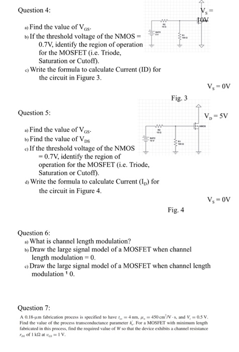

Question 4: W a Find the value of Vas b If the threshold voltage of the NMOS = 0.7V, identify the region of operation for the MOSFET (i.e. Triode Saturation or Cutoff) e Write the formula to calculate Current (ID) for the circuit in Figure 3. Fig. 3 Question 5: V=5V ww a Find the value of VGS b) Find the value of Vps e) If the threshold voltage of the NMOS 0.7V, identify the region of operation for the MOSFET (i.e. Triode Saturation or Cutoff) d) Write the formula to calculate Current (Ip) for the circuit in Figure 4. Fig. 4 Question 6 a) What is channel length modulation? b) Draw the large signal model of a MOSFET when channel length modulation 0. e) Draw the large signal model of a MOSFET when channel length modulation 0 Question 7: A 0.18-um fabrication process is specified to have 4 nm, p,= 450 cmN-s, and V, 0.5 V Find the value of the process transconductance parameter . For a MOSFET with minimum length fabricated in this process, find the required value of W so that the device exhibits a channel resistance r of I k2 at IV.
Lecture Summary We discussed MOSFET biasing and different regions of operations. We further discussed IV characteristics of ideal and non-ideal MOSFET . Channel length modulation and effect of channel length modulation on current ID was also discussed during the lectures.
Homework Answers
Question number 4 and 5 have been solved here with proper explanation.

 In problem 4, though the value
of VD is not given or clearly mentioned, but in the
above calculation, it is shown that VGS <
Vt because VGS = -10 Volts
and Vt = 0.7 Volts. So the NMOS in figure 4 is in
Cutoff region. No
current is flowing through the NMOS.
In problem 4, though the value
of VD is not given or clearly mentioned, but in the
above calculation, it is shown that VGS <
Vt because VGS = -10 Volts
and Vt = 0.7 Volts. So the NMOS in figure 4 is in
Cutoff region. No
current is flowing through the NMOS.


Add Answer to:
Vs 82 BATZ IOS = eration rrent (ID) for Fig. 3 VD 5V NMOS 10 0 BAT2 R1 1000 IOS . Triode, rrent (In) for Fig...
Question 2: a) Find the value of Vgs? b) If the threshold voltage of the NMOS 0.7V, identify the region o...
 Question 2: a) Find the value of Vgs? b) If the threshold voltage of the NMOS 0.7V, identify the region of operation for the MOSFET (i.e. Triode Saturation or Cutoff) v,= 10V SATE e) Write the formula to calculate Current (ID) for the circuit in Figure 1 Fig. 1 Question 3: a) Find the value of Vgs* b) If the threshold voltage of the NMOS 0.7V, identify the region of operation for the MOSFET (i.e. Triode, Saturation or Cutoff) c)...
Lecture Summary We discussed MOSFET biasing and different regions of operations. We further discussed IV character...
 Lecture Summary We discussed MOSFET biasing and different regions of operations. We further discussed IV characteristicss of ideal and non-ideal MOSFETS. Channel length modulation and effect of channel length modulation on current ID was also discussed during the lectures. Quentinductor and PN junction is also introduced in the lectures. Draw IV characteristics of an ideal diode. b Draw IV characteristics of a non-ideal diode with Vt 0.4V e Draw IV characteristics of an ideal MOSFET al d) Draw IV characteristics...
Design a common-source MOSFET amplifier such that - Rg is a multiple of 10 - Id...
Design a common-source MOSFET amplifier such that - Rg is a multiple of 10 - Id = 0.52 mA - the amplifier input resistance is in the range of mega ohms - | Avo | = 16.7 V/V - RL = 20k - Vsig has a 2kHz frequency - Rsig = 400k, and is the input and the MOSFET has: Vt = 0.8V k = 5 mA/V^2 VA = 80 V Assume capacitors are shorted in the signal circuit and...
2. (36% ) In Fig. 2, the device parameters and (W/L) ratios for Q1-Q3 are given...
 2. (36% ) In Fig. 2, the device parameters and (W/L) ratios for Q1-Q3 are given below (WIL), 2 (W/L)2-2 (W/L); (a) (10%) If IREF-2nA, find VD3 and VS3 and verify if Q3 is in saturation. Ignore the channel length modulation for DC analysis. Note: DC Vc30 (b) (12%) Draw the "small signal" circuit for the complete +10 V amplifier. Based on the circuit, derive the AC voltage gain vo/vi in terms gm, ro and RD (please use appropriate subscripts...
 Question 2: a) Find the value of Vgs? b) If the threshold voltage of the NMOS 0.7V, identify the region of operation for the MOSFET (i.e. Triode Saturation or Cutoff) v,= 10V SATE e) Write the formula to calculate Current (ID) for the circuit in Figure 1 Fig. 1 Question 3: a) Find the value of Vgs* b) If the threshold voltage of the NMOS 0.7V, identify the region of operation for the MOSFET (i.e. Triode, Saturation or Cutoff) c)...
 Lecture Summary We discussed MOSFET biasing and different regions of operations. We further discussed IV characteristicss of ideal and non-ideal MOSFETS. Channel length modulation and effect of channel length modulation on current ID was also discussed during the lectures. Quentinductor and PN junction is also introduced in the lectures. Draw IV characteristics of an ideal diode. b Draw IV characteristics of a non-ideal diode with Vt 0.4V e Draw IV characteristics of an ideal MOSFET al d) Draw IV characteristics...
 2. (36% ) In Fig. 2, the device parameters and (W/L) ratios for Q1-Q3 are given below (WIL), 2 (W/L)2-2 (W/L); (a) (10%) If IREF-2nA, find VD3 and VS3 and verify if Q3 is in saturation. Ignore the channel length modulation for DC analysis. Note: DC Vc30 (b) (12%) Draw the "small signal" circuit for the complete +10 V amplifier. Based on the circuit, derive the AC voltage gain vo/vi in terms gm, ro and RD (please use appropriate subscripts...
Most questions answered within 3 hours.
-
An electric field at a spatial point does NOT depend on: (Choose
all the answers)
a....
asked 2 seconds ago -
As you being to perform the network-mapping phase of the
scenario, you have been asked what...
asked 3 minutes ago -
Find the sample size, n, needed to estimate the percentage of
adults who have consulted fortune...
asked 21 minutes ago -
When the relationship is perfect, the regression of Y on X is a
perfect straight line....
asked 36 minutes ago -
What would be the balanced equation for the addition of
concentrated hydrochloric acid to cobalt chloride?...
asked 41 minutes ago -
Regarding a constructive discharge claim, whether an employee's
working conditions were so intolerable that he/she had...
asked 41 minutes ago -
Use a z -Table to find the specified area.
Between the mean and 3.01 deviations from...
asked 43 minutes ago -
If the rate constant for a particular reaction
triples between 35 °C and
70 °C, calculate...
asked 49 minutes ago -
if a magnetic field of 0.634 T is measured a distance of 0.009 m
away from...
asked 53 minutes ago -
In
the past, Ben has been able to hit a baseball at the batting cage
20%...
asked 56 minutes ago -
"Function does not take 0 arguments". I keep getting this error
for my last line of...
asked 56 minutes ago -
C++
What are the advantages of having a full copy of an object over
just having...
asked 57 minutes ago