
Ri Rp R 8mVgs Vo Rs Vin + v(t)
Homework Answers
Add Answer to:
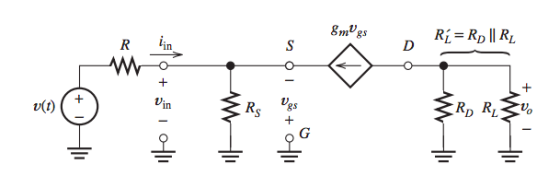
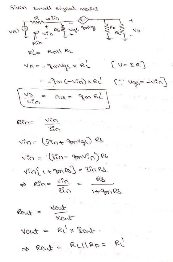
Exercise 12.13 Derive expressions for the voltage gain, input resistance, and output resistance of the common-gate...
Answer full question oe stage 6.6 Analyze a common-gate JFET amplifier as shown in Figure 6.37(a)...
 Answer full question
oe stage 6.6 Analyze a common-gate JFET amplifier as shown in Figure 6.37(a) when VDD-12 V, Vss = o. R, = 205 kQ, R2= 8 MQ, Rs = 500 Ω, RD= 2 ks2. Rlad-4 kf1/w" 2.8 mA, and the transistor has loss = 7 mA and VP-3 V. Determine A" A" and Rin for the circuit.
Answer full question
oe stage 6.6 Analyze a common-gate JFET amplifier as shown in Figure 6.37(a) when VDD-12 V, Vss = o. R, = 205 kQ, R2= 8 MQ, Rs = 500 Ω, RD= 2 ks2. Rlad-4 kf1/w" 2.8 mA, and the transistor has loss = 7 mA and VP-3 V. Determine A" A" and Rin for the circuit.
VDD RD RG1 out Vin G2 Figure 3 Design your own common source amplifier based on...
 VDD RD RG1 out Vin G2 Figure 3 Design your own common source amplifier based on Figure 3. You need an input resistance Rin 1M2. Make VD 2Voo/3, Vs Voo/3. Use VG 5 [V]. VoD 10 [V] a. Draw the small signal equivalent circuit b. Find RG1, and RG2, and lo c. Choose values of Ro, and Rs d. Find gm, and Av-Vout/Vin
In the CS amplifier shown in the figure above, Rsig = 20 kΩ amplifier input resistance...
 In the CS amplifier shown in the figure above, Rsig =
20 kΩ amplifier input resistance Rin = 80 kΩ,
Cgs=2pF, Cgd= 0.5pF, gm=2mA/V,
ro= 80 kΩ , RD = 5 kΩ, and RL = 10
kΩ. (π = 3.14)
a) Determine high frequency cut-off fH.
(Use Miller Approximation. Use . as the
decimal point. Answer in MHz; for 7.89MHz write 7.89
only.)
VOD RD V RIS R CS V Ro In the CS amplifier shown in the figure above....
In the CS amplifier shown in the figure above, Rsig =
20 kΩ amplifier input resistance Rin = 80 kΩ,
Cgs=2pF, Cgd= 0.5pF, gm=2mA/V,
ro= 80 kΩ , RD = 5 kΩ, and RL = 10
kΩ. (π = 3.14)
a) Determine high frequency cut-off fH.
(Use Miller Approximation. Use . as the
decimal point. Answer in MHz; for 7.89MHz write 7.89
only.)
VOD RD V RIS R CS V Ro In the CS amplifier shown in the figure above....
Problem 1130 pts 1. [12 pts] For the circuit shown in Fig. 1, istance Rm when the switch is open. What type of voltage gain Vo/Vin and the input resistance Rin when the switch is close. What type of...
 Problem 1130 pts 1. [12 pts] For the circuit shown in Fig. 1, istance Rm when the switch is open. What type of voltage gain Vo/Vin and the input resistance Rin when the switch is close. What type of a) Find the voltage gain val vin and the input resistance Rin when the switch is open b) Find the amplifier is this? amplifier is this? tin vo R Fig. 1 [18 pts] Design a circuit that implements the following: Vo(t)...
Please answer clearly Question 2 The amplifier shown in Figure 2 has the following parameters: Kn(W/L)-1 mA/V2, V-1 V Determine a) Voltage gain (Vo/vi) b) Input resistance (R) c) Output resistance (R...
 Please answer clearly
Question 2 The amplifier shown in Figure 2 has the following parameters: Kn(W/L)-1 mA/V2, V-1 V Determine a) Voltage gain (Vo/vi) b) Input resistance (R) c) Output resistance (Ro) d) Maximum output voltage swing so as the amplifier stays in saturation mode. Assume VDD-20 V, R1-2.5 ΚΩ, R2-1KQ, R3-0.5 ΚΩ, R4-5 MQ, R5_1ΜΩ. R4 R1 R5 R2 Ro R3
Question 2 The amplifier shown in Figure 2 has the following parameters: Kn(W/L)-1 mA/V2, V-1 V Determine a)...
Please answer clearly
Question 2 The amplifier shown in Figure 2 has the following parameters: Kn(W/L)-1 mA/V2, V-1 V Determine a) Voltage gain (Vo/vi) b) Input resistance (R) c) Output resistance (Ro) d) Maximum output voltage swing so as the amplifier stays in saturation mode. Assume VDD-20 V, R1-2.5 ΚΩ, R2-1KQ, R3-0.5 ΚΩ, R4-5 MQ, R5_1ΜΩ. R4 R1 R5 R2 Ro R3
Question 2 The amplifier shown in Figure 2 has the following parameters: Kn(W/L)-1 mA/V2, V-1 V Determine a)...
The circuit 3-The circuit of problem # 2 is subjected to a small ac input by the signal generator. By neglecting the voltage drop across the coupling and bypass capacitors, determine the small signa...
 The circuit
3-The circuit of problem # 2 is subjected to a small ac input by the signal generator. By neglecting the voltage drop across the coupling and bypass capacitors, determine the small signal voltage gain Vo/ Vì = Avi , input resistance Ri-vi / ii and the output resistance Ro external to R Avi= Ri= , Ro The accompanying circuit shows a 4-resistor biased JFET transistor Determine the values of Rp and Rs so that the Q-point is equal...
The circuit
3-The circuit of problem # 2 is subjected to a small ac input by the signal generator. By neglecting the voltage drop across the coupling and bypass capacitors, determine the small signal voltage gain Vo/ Vì = Avi , input resistance Ri-vi / ii and the output resistance Ro external to R Avi= Ri= , Ro The accompanying circuit shows a 4-resistor biased JFET transistor Determine the values of Rp and Rs so that the Q-point is equal...
Vdd RL VO OL vin Rg ww The figure shows the circuit diagram of a common...
 Vdd RL VO OL vin Rg ww The figure shows the circuit diagram of a common source amplifier using a JFET supplied by an ideal sinusoidal signal source vin of variable frequency. The values of the circuit components are given as follows; Rg = 560k, RL = 1.5k, ro = infinity, C = 0.01 microfarads, gm = 7.0mA/Volt. At a frequency of 50 Hz it is determined that the magnitude of the gain vo/vin is nearest to which of the...
URGENT The NMOS in the shown figure has Vt = 0.8V, kn = 5 mA/V2, and...
 URGENT
The NMOS in the shown figure has Vt = 0.8V, kn = 5 mA/V2, and VA = 40 V. The circuit also has Vdd = 5V, VSS = -5V, RG = RLD = 1 M2, and RLS = 0 A. [3 marks] Neglecting the channel length modulation effect, find the value of Rs so that the NMOS operates in saturation with Ip = 0.4 mA B. [2 marks] Neglecting the channel length modulation effect, find the largest possible value...
URGENT
The NMOS in the shown figure has Vt = 0.8V, kn = 5 mA/V2, and VA = 40 V. The circuit also has Vdd = 5V, VSS = -5V, RG = RLD = 1 M2, and RLS = 0 A. [3 marks] Neglecting the channel length modulation effect, find the value of Rs so that the NMOS operates in saturation with Ip = 0.4 mA B. [2 marks] Neglecting the channel length modulation effect, find the largest possible value...
2.34. Consider the common-emitter amplifier on the right. (a)Draw a small-signal equivalent circuit using the T-model without the B1 Cci output resistance (b)Find an expression for the input resistan...
 2.34. Consider the common-emitter amplifier on the right. (a)Draw a small-signal equivalent circuit using the T-model without the B1 Cci output resistance (b)Find an expression for the input resistance Rin. (c)Find an expression for the output resistance Ro. (d) Find an expression for the lower cut-off frequency Vi Re sig 82 C, (RE-R) in associated with Cci. (d)Find expressions for the two gains vo/v, and v/Vsig CI.
2.34. Consider the common-emitter amplifier on the right. (a)Draw a small-signal equivalent circuit...
2.34. Consider the common-emitter amplifier on the right. (a)Draw a small-signal equivalent circuit using the T-model without the B1 Cci output resistance (b)Find an expression for the input resistance Rin. (c)Find an expression for the output resistance Ro. (d) Find an expression for the lower cut-off frequency Vi Re sig 82 C, (RE-R) in associated with Cci. (d)Find expressions for the two gains vo/v, and v/Vsig CI.
2.34. Consider the common-emitter amplifier on the right. (a)Draw a small-signal equivalent circuit...
in great detail plz 1. Figure la shows a CG amplifier with a signal source and...
 in great detail plz
1. Figure la shows a CG amplifier with a signal source and loaded with a resistance Ru. Do NOT ignore ro of Q. (50pt) OB Vio o+ Vsig : + 6 G .sis 5 Figure la Figure 1b rotre (a) Derive an expression for Rin (5pt) Hgmro (b) Noting that the current through R is equal to the input current i, derive an expression for the overall voltage gain No/Vsig (5pt) (c) Find Rin and Vo/Vsig...
in great detail plz
1. Figure la shows a CG amplifier with a signal source and loaded with a resistance Ru. Do NOT ignore ro of Q. (50pt) OB Vio o+ Vsig : + 6 G .sis 5 Figure la Figure 1b rotre (a) Derive an expression for Rin (5pt) Hgmro (b) Noting that the current through R is equal to the input current i, derive an expression for the overall voltage gain No/Vsig (5pt) (c) Find Rin and Vo/Vsig...
 Answer full question
oe stage 6.6 Analyze a common-gate JFET amplifier as shown in Figure 6.37(a) when VDD-12 V, Vss = o. R, = 205 kQ, R2= 8 MQ, Rs = 500 Ω, RD= 2 ks2. Rlad-4 kf1/w" 2.8 mA, and the transistor has loss = 7 mA and VP-3 V. Determine A" A" and Rin for the circuit.
Answer full question
oe stage 6.6 Analyze a common-gate JFET amplifier as shown in Figure 6.37(a) when VDD-12 V, Vss = o. R, = 205 kQ, R2= 8 MQ, Rs = 500 Ω, RD= 2 ks2. Rlad-4 kf1/w" 2.8 mA, and the transistor has loss = 7 mA and VP-3 V. Determine A" A" and Rin for the circuit.
 VDD RD RG1 out Vin G2 Figure 3 Design your own common source amplifier based on Figure 3. You need an input resistance Rin 1M2. Make VD 2Voo/3, Vs Voo/3. Use VG 5 [V]. VoD 10 [V] a. Draw the small signal equivalent circuit b. Find RG1, and RG2, and lo c. Choose values of Ro, and Rs d. Find gm, and Av-Vout/Vin
 In the CS amplifier shown in the figure above, Rsig =
20 kΩ amplifier input resistance Rin = 80 kΩ,
Cgs=2pF, Cgd= 0.5pF, gm=2mA/V,
ro= 80 kΩ , RD = 5 kΩ, and RL = 10
kΩ. (π = 3.14)
a) Determine high frequency cut-off fH.
(Use Miller Approximation. Use . as the
decimal point. Answer in MHz; for 7.89MHz write 7.89
only.)
VOD RD V RIS R CS V Ro In the CS amplifier shown in the figure above....
In the CS amplifier shown in the figure above, Rsig =
20 kΩ amplifier input resistance Rin = 80 kΩ,
Cgs=2pF, Cgd= 0.5pF, gm=2mA/V,
ro= 80 kΩ , RD = 5 kΩ, and RL = 10
kΩ. (π = 3.14)
a) Determine high frequency cut-off fH.
(Use Miller Approximation. Use . as the
decimal point. Answer in MHz; for 7.89MHz write 7.89
only.)
VOD RD V RIS R CS V Ro In the CS amplifier shown in the figure above....
 Problem 1130 pts 1. [12 pts] For the circuit shown in Fig. 1, istance Rm when the switch is open. What type of voltage gain Vo/Vin and the input resistance Rin when the switch is close. What type of a) Find the voltage gain val vin and the input resistance Rin when the switch is open b) Find the amplifier is this? amplifier is this? tin vo R Fig. 1 [18 pts] Design a circuit that implements the following: Vo(t)...
 Please answer clearly
Question 2 The amplifier shown in Figure 2 has the following parameters: Kn(W/L)-1 mA/V2, V-1 V Determine a) Voltage gain (Vo/vi) b) Input resistance (R) c) Output resistance (Ro) d) Maximum output voltage swing so as the amplifier stays in saturation mode. Assume VDD-20 V, R1-2.5 ΚΩ, R2-1KQ, R3-0.5 ΚΩ, R4-5 MQ, R5_1ΜΩ. R4 R1 R5 R2 Ro R3
Question 2 The amplifier shown in Figure 2 has the following parameters: Kn(W/L)-1 mA/V2, V-1 V Determine a)...
Please answer clearly
Question 2 The amplifier shown in Figure 2 has the following parameters: Kn(W/L)-1 mA/V2, V-1 V Determine a) Voltage gain (Vo/vi) b) Input resistance (R) c) Output resistance (Ro) d) Maximum output voltage swing so as the amplifier stays in saturation mode. Assume VDD-20 V, R1-2.5 ΚΩ, R2-1KQ, R3-0.5 ΚΩ, R4-5 MQ, R5_1ΜΩ. R4 R1 R5 R2 Ro R3
Question 2 The amplifier shown in Figure 2 has the following parameters: Kn(W/L)-1 mA/V2, V-1 V Determine a)...
 The circuit
3-The circuit of problem # 2 is subjected to a small ac input by the signal generator. By neglecting the voltage drop across the coupling and bypass capacitors, determine the small signal voltage gain Vo/ Vì = Avi , input resistance Ri-vi / ii and the output resistance Ro external to R Avi= Ri= , Ro The accompanying circuit shows a 4-resistor biased JFET transistor Determine the values of Rp and Rs so that the Q-point is equal...
The circuit
3-The circuit of problem # 2 is subjected to a small ac input by the signal generator. By neglecting the voltage drop across the coupling and bypass capacitors, determine the small signal voltage gain Vo/ Vì = Avi , input resistance Ri-vi / ii and the output resistance Ro external to R Avi= Ri= , Ro The accompanying circuit shows a 4-resistor biased JFET transistor Determine the values of Rp and Rs so that the Q-point is equal...
 Vdd RL VO OL vin Rg ww The figure shows the circuit diagram of a common source amplifier using a JFET supplied by an ideal sinusoidal signal source vin of variable frequency. The values of the circuit components are given as follows; Rg = 560k, RL = 1.5k, ro = infinity, C = 0.01 microfarads, gm = 7.0mA/Volt. At a frequency of 50 Hz it is determined that the magnitude of the gain vo/vin is nearest to which of the...
 URGENT
The NMOS in the shown figure has Vt = 0.8V, kn = 5 mA/V2, and VA = 40 V. The circuit also has Vdd = 5V, VSS = -5V, RG = RLD = 1 M2, and RLS = 0 A. [3 marks] Neglecting the channel length modulation effect, find the value of Rs so that the NMOS operates in saturation with Ip = 0.4 mA B. [2 marks] Neglecting the channel length modulation effect, find the largest possible value...
URGENT
The NMOS in the shown figure has Vt = 0.8V, kn = 5 mA/V2, and VA = 40 V. The circuit also has Vdd = 5V, VSS = -5V, RG = RLD = 1 M2, and RLS = 0 A. [3 marks] Neglecting the channel length modulation effect, find the value of Rs so that the NMOS operates in saturation with Ip = 0.4 mA B. [2 marks] Neglecting the channel length modulation effect, find the largest possible value...
 2.34. Consider the common-emitter amplifier on the right. (a)Draw a small-signal equivalent circuit using the T-model without the B1 Cci output resistance (b)Find an expression for the input resistance Rin. (c)Find an expression for the output resistance Ro. (d) Find an expression for the lower cut-off frequency Vi Re sig 82 C, (RE-R) in associated with Cci. (d)Find expressions for the two gains vo/v, and v/Vsig CI.
2.34. Consider the common-emitter amplifier on the right. (a)Draw a small-signal equivalent circuit...
2.34. Consider the common-emitter amplifier on the right. (a)Draw a small-signal equivalent circuit using the T-model without the B1 Cci output resistance (b)Find an expression for the input resistance Rin. (c)Find an expression for the output resistance Ro. (d) Find an expression for the lower cut-off frequency Vi Re sig 82 C, (RE-R) in associated with Cci. (d)Find expressions for the two gains vo/v, and v/Vsig CI.
2.34. Consider the common-emitter amplifier on the right. (a)Draw a small-signal equivalent circuit...
 in great detail plz
1. Figure la shows a CG amplifier with a signal source and loaded with a resistance Ru. Do NOT ignore ro of Q. (50pt) OB Vio o+ Vsig : + 6 G .sis 5 Figure la Figure 1b rotre (a) Derive an expression for Rin (5pt) Hgmro (b) Noting that the current through R is equal to the input current i, derive an expression for the overall voltage gain No/Vsig (5pt) (c) Find Rin and Vo/Vsig...
in great detail plz
1. Figure la shows a CG amplifier with a signal source and loaded with a resistance Ru. Do NOT ignore ro of Q. (50pt) OB Vio o+ Vsig : + 6 G .sis 5 Figure la Figure 1b rotre (a) Derive an expression for Rin (5pt) Hgmro (b) Noting that the current through R is equal to the input current i, derive an expression for the overall voltage gain No/Vsig (5pt) (c) Find Rin and Vo/Vsig...
Most questions answered within 3 hours.
-
Which of the following pairs of ions have the same electron
configuration?
I: Br− and Se2−...
asked 1 hour ago -
The Foremost Composite Materials Company is planning a two-day
sales conference for October 19-20. The conference...
asked 1 hour ago -
3) Illustrate the observed pattern of relatedness of organisms
versus adaptations to specific conditions. This means...
asked 2 hours ago -
In winter a lake has a 0.35 m thick ice layer over 1.10 m of
water....
asked 3 hours ago -
Assuming the following has been encrypted with a Vigenere cipher
below, use the method(s) and assumptions...
asked 3 hours ago -
How would I use switch statements to write a program that will
take an input of...
asked 3 hours ago -
Imagine a reaction in which methane gas combusts at a constant
pressure of 1 atm and...
asked 3 hours ago -
Two parallel wires (each 12 m in length) are separated by a
distance of 0.065 m...
asked 3 hours ago -
Suppose there were three masses at the corner of uniform
equilateral triangle. The masses are m1...
asked 3 hours ago -
Situation: A building that is 618 m above the ground floor. How
many times would a...
asked 3 hours ago -
help me and discuss one successful and one
unsuccessful international company/busines in Indonesia.whyit
succeed and why...
asked 3 hours ago -
I- Choose the best answer
Which of the following statements about the structure and
packaging of...
asked 3 hours ago