D Flip-Flops Include the symbol and characteristic table of a 1-bit rising edge D flip-flop Write...
D Flip-Flops
- Include the symbol and characteristic table of a 1-bit rising edge D flip-flop
- Write a Verilog module called dflipflop to implement a simple one-bit D flip Flop with input of data and clock and 1-bit output data
Homework Answers
Solution :-
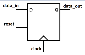
DFF Block Diagram is shown below:-
Truth Table for 1 bit DFF:-

Verilog code for 1 bit DFF is mentioned below:-
//DFF module
module dff (
input clk, // Clock Input
input rst, // Reset Input
input data_in, // Input Data
output reg data_out // Output Data
);
always @ (posedge clk) // triggers at the postive edge of the
clock
begin
if (rst) // Synchronous Active High reset
data_out <= 1'b0;
else
data_out <= data_in; // When reset is not present then it
forward the input data to output
end
endmodule
Add Answer to:
D Flip-Flops
Include the symbol and characteristic table of a 1-bit rising
edge D flip-flop
Write...
Use the Quartus Prime Text Editor to implement a behavioral model of the D flip-flop described ab...
 Use the Quartus Prime Text Editor to implement a behavioral
model of the D flip-flop described above in a file named
d_flops.sv. Specify the D flip-flop’s module according to the
interface specification given in the table below.
Port
Mode
Data Type
Size
Description
RST
in
logic
1-bit
Active high asynchronous reset
CLK
in
logic
1-bit
Synchronizing clock signal
EN
in
logic
1-bit
Synchronous clock enable
D
in
logic
1-bit
Synchronous data input
Q
out
logic
1-bit
Current/present state
Qbar
out...
Use the Quartus Prime Text Editor to implement a behavioral
model of the D flip-flop described above in a file named
d_flops.sv. Specify the D flip-flop’s module according to the
interface specification given in the table below.
Port
Mode
Data Type
Size
Description
RST
in
logic
1-bit
Active high asynchronous reset
CLK
in
logic
1-bit
Synchronizing clock signal
EN
in
logic
1-bit
Synchronous clock enable
D
in
logic
1-bit
Synchronous data input
Q
out
logic
1-bit
Current/present state
Qbar
out...
3. Answer the following questions about a data flip-flop (D-Flip Flop): a) (4 ps) Write the VHDL required to define a rising-edge triggered (RET) D-Flip Flop with additional clock enable (CEN) an...
 3. Answer the following questions about a data flip-flop (D-Flip Flop): a) (4 ps) Write the VHDL required to define a rising-edge triggered (RET) D-Flip Flop with additional clock enable (CEN) and reset inputs. Your reset may be synchronous or asynchronous. Assume any input, output, or signal variables that you require have already been declared in VHDL (you do not have to write the declarations for these) b) [I pal ls your reset syachronous or asynchronous for the D-Flip Flop...
VHDL Using D-flip-flops, generate an 8-bit LFSR (Linear Feedbaclk Shift-Register). For every bit, include a Binary Cont...
 VHDL
Using D-flip-flops, generate an 8-bit LFSR (Linear Feedbaclk Shift-Register). For every bit, include a Binary Control (BC) value that can turn the contribution of the flip-flop output to the XOR input on or off (1 for ON, 0 for OFF). For the 8-bit LFSR include a 7-bit ge- neric BIT_VECTOR that can configure contribution of LFSR flip-flops to the LFSR feedback. The right-most flip-flop output has no XOR, and the left-most flip-flop input is fed by the feedback line...
VHDL
Using D-flip-flops, generate an 8-bit LFSR (Linear Feedbaclk Shift-Register). For every bit, include a Binary Control (BC) value that can turn the contribution of the flip-flop output to the XOR input on or off (1 for ON, 0 for OFF). For the 8-bit LFSR include a 7-bit ge- neric BIT_VECTOR that can configure contribution of LFSR flip-flops to the LFSR feedback. The right-most flip-flop output has no XOR, and the left-most flip-flop input is fed by the feedback line...
All flip flops are positive-edge triggered. Assume each flip flop starts at 0.
 All flip flops are
positive-edge triggered. Assume each flip flop starts at 0.
Problem 11: (8 pts) For the following circuit, complete the timing diagram for the state of each flip flop and the output, where shown. All flip flops are positive-edge triggered. Assume each flip flop starts at 0. J-K FF TFF CLK PRE CLR PRE CLR CLR回 Clock CLR
Problem 11: (8 pts) For the following circuit, complete the timing diagram for the state of each flip flop...
All flip flops are
positive-edge triggered. Assume each flip flop starts at 0.
Problem 11: (8 pts) For the following circuit, complete the timing diagram for the state of each flip flop and the output, where shown. All flip flops are positive-edge triggered. Assume each flip flop starts at 0. J-K FF TFF CLK PRE CLR PRE CLR CLR回 Clock CLR
Problem 11: (8 pts) For the following circuit, complete the timing diagram for the state of each flip flop...
1. The D Flip-Flop ) Look for the datasheet of the 7474 D flip-flop and wire it on the breadboard...
 1. The D Flip-Flop ) Look for the datasheet of the 7474 D flip-flop and wire it on the breadboard making sure to supply 5V to both Preset and Clear. Utilize the function generator to provide a Clock signal of 1 Hz: i) Press AMPL and set value to 5 Vpp ii) Press FREQ and set value to 1 Hz ili) Press OFFSET and set value to 2.5 V This Clock signal will be the same for all circuits in...
WRITE THE CODE IN VERILOG: Instead of using Registers, USE D FLIP FLOPS and a clock....
 WRITE THE CODE IN VERILOG: Instead of using Registers, USE D
FLIP FLOPS and a clock. Include the logic for a reset
A sequential circuit with three D flip-flops A, B, and C, a trigger x, and an output z1, and zo. On this state machine diagram, the label of the states are in the order of (ABC), the transition is the one bit x, and the output is under the forward slash. x/z1zo. The start state is 001 0/01...
WRITE THE CODE IN VERILOG: Instead of using Registers, USE D
FLIP FLOPS and a clock. Include the logic for a reset
A sequential circuit with three D flip-flops A, B, and C, a trigger x, and an output z1, and zo. On this state machine diagram, the label of the states are in the order of (ABC), the transition is the one bit x, and the output is under the forward slash. x/z1zo. The start state is 001 0/01...
Design a double edge-triggered D flip-flop using multiplexers only. The output of the flip-flop Q should...
Design a double edge-triggered D flip-flop using multiplexers only. The output of the flip-flop Q should “sample” the value of the input D on both rising (+ve) and falling (-ve) edges of the clock CLK. Provide detailed solution and explanation.
Design a double edge-triggered D flip-flop. The output of the flip-flop Q should "sample" the value...
 Design a double edge-triggered D flip-flop. The output of the flip-flop Q should "sample" the value of the input D on both rising (+ve) and falling (-ve) edges of the clock CLK. Design an FSM counter that counts the sequence: 00, 11, 01, 10,00, 11, ..
10.21 Write a behavioral Verilog module vrDnegEc for a negative-edge-triggered D flip-flop with enable and asynchronous...
 10.21 Write a behavioral Verilog module vrDnegEc for a negative-edge-triggered D flip-flop with enable and asynchronous active-low clear. Also write a test bench that instantiates your flip-flop and exercises its operation for a comprehensive input sequence.
Q D Clock Clk Q Clock Qb Q Qa Q Q Multiple type of flip-flops Circuit...
 Q D Clock Clk Q Clock Qb Q Qa Q Q Multiple type of flip-flops Circuit The figure above shows a circuit that use three different types of D flip-flops: a) D latch b) Rising-edge D flip-flop c) Falling-edge flip-flop For each one of the flip-flops enter their output for the times t1.t2.t3.t4 Assume that initially all outputs are '0' D
 Use the Quartus Prime Text Editor to implement a behavioral
model of the D flip-flop described above in a file named
d_flops.sv. Specify the D flip-flop’s module according to the
interface specification given in the table below.
Port
Mode
Data Type
Size
Description
RST
in
logic
1-bit
Active high asynchronous reset
CLK
in
logic
1-bit
Synchronizing clock signal
EN
in
logic
1-bit
Synchronous clock enable
D
in
logic
1-bit
Synchronous data input
Q
out
logic
1-bit
Current/present state
Qbar
out...
Use the Quartus Prime Text Editor to implement a behavioral
model of the D flip-flop described above in a file named
d_flops.sv. Specify the D flip-flop’s module according to the
interface specification given in the table below.
Port
Mode
Data Type
Size
Description
RST
in
logic
1-bit
Active high asynchronous reset
CLK
in
logic
1-bit
Synchronizing clock signal
EN
in
logic
1-bit
Synchronous clock enable
D
in
logic
1-bit
Synchronous data input
Q
out
logic
1-bit
Current/present state
Qbar
out...
 3. Answer the following questions about a data flip-flop (D-Flip Flop): a) (4 ps) Write the VHDL required to define a rising-edge triggered (RET) D-Flip Flop with additional clock enable (CEN) and reset inputs. Your reset may be synchronous or asynchronous. Assume any input, output, or signal variables that you require have already been declared in VHDL (you do not have to write the declarations for these) b) [I pal ls your reset syachronous or asynchronous for the D-Flip Flop...
 VHDL
Using D-flip-flops, generate an 8-bit LFSR (Linear Feedbaclk Shift-Register). For every bit, include a Binary Control (BC) value that can turn the contribution of the flip-flop output to the XOR input on or off (1 for ON, 0 for OFF). For the 8-bit LFSR include a 7-bit ge- neric BIT_VECTOR that can configure contribution of LFSR flip-flops to the LFSR feedback. The right-most flip-flop output has no XOR, and the left-most flip-flop input is fed by the feedback line...
VHDL
Using D-flip-flops, generate an 8-bit LFSR (Linear Feedbaclk Shift-Register). For every bit, include a Binary Control (BC) value that can turn the contribution of the flip-flop output to the XOR input on or off (1 for ON, 0 for OFF). For the 8-bit LFSR include a 7-bit ge- neric BIT_VECTOR that can configure contribution of LFSR flip-flops to the LFSR feedback. The right-most flip-flop output has no XOR, and the left-most flip-flop input is fed by the feedback line...
 All flip flops are
positive-edge triggered. Assume each flip flop starts at 0.
Problem 11: (8 pts) For the following circuit, complete the timing diagram for the state of each flip flop and the output, where shown. All flip flops are positive-edge triggered. Assume each flip flop starts at 0. J-K FF TFF CLK PRE CLR PRE CLR CLR回 Clock CLR
Problem 11: (8 pts) For the following circuit, complete the timing diagram for the state of each flip flop...
All flip flops are
positive-edge triggered. Assume each flip flop starts at 0.
Problem 11: (8 pts) For the following circuit, complete the timing diagram for the state of each flip flop and the output, where shown. All flip flops are positive-edge triggered. Assume each flip flop starts at 0. J-K FF TFF CLK PRE CLR PRE CLR CLR回 Clock CLR
Problem 11: (8 pts) For the following circuit, complete the timing diagram for the state of each flip flop...
 1. The D Flip-Flop ) Look for the datasheet of the 7474 D flip-flop and wire it on the breadboard making sure to supply 5V to both Preset and Clear. Utilize the function generator to provide a Clock signal of 1 Hz: i) Press AMPL and set value to 5 Vpp ii) Press FREQ and set value to 1 Hz ili) Press OFFSET and set value to 2.5 V This Clock signal will be the same for all circuits in...
 WRITE THE CODE IN VERILOG: Instead of using Registers, USE D
FLIP FLOPS and a clock. Include the logic for a reset
A sequential circuit with three D flip-flops A, B, and C, a trigger x, and an output z1, and zo. On this state machine diagram, the label of the states are in the order of (ABC), the transition is the one bit x, and the output is under the forward slash. x/z1zo. The start state is 001 0/01...
WRITE THE CODE IN VERILOG: Instead of using Registers, USE D
FLIP FLOPS and a clock. Include the logic for a reset
A sequential circuit with three D flip-flops A, B, and C, a trigger x, and an output z1, and zo. On this state machine diagram, the label of the states are in the order of (ABC), the transition is the one bit x, and the output is under the forward slash. x/z1zo. The start state is 001 0/01...
 Design a double edge-triggered D flip-flop. The output of the flip-flop Q should "sample" the value of the input D on both rising (+ve) and falling (-ve) edges of the clock CLK. Design an FSM counter that counts the sequence: 00, 11, 01, 10,00, 11, ..
 10.21 Write a behavioral Verilog module vrDnegEc for a negative-edge-triggered D flip-flop with enable and asynchronous active-low clear. Also write a test bench that instantiates your flip-flop and exercises its operation for a comprehensive input sequence.
 Q D Clock Clk Q Clock Qb Q Qa Q Q Multiple type of flip-flops Circuit The figure above shows a circuit that use three different types of D flip-flops: a) D latch b) Rising-edge D flip-flop c) Falling-edge flip-flop For each one of the flip-flops enter their output for the times t1.t2.t3.t4 Assume that initially all outputs are '0' D
Most questions answered within 3 hours.
-
3) What are the typical social structures in a global city?
asked 19 minutes ago -
Luther Corporation
Consolidated Balance Sheet
December 31, 2019 and 2018 (in $ millions)
Assets
2019
2018...
asked 21 minutes ago -
(Expected rate of return and risk) Carter Inc. is evaluating a
security. Calculate the investment’s expected...
asked 3 hours ago -
What specific indicators can point to lack of progress for
African Americans in American society?
asked 4 hours ago -
1-The Electrons in a beam are moving at 2.7×10⁸ m/s in an
electric field of 15000...
asked 4 hours ago -
A gas tank is a vertical cylinder. It has a radius of 1m, a
height of...
asked 4 hours ago -
Accent Software faces the following conditions. All of these
support Accent’s use of a market-penetration pricing...
asked 5 hours ago -
A mathematically inclined friend emails you the following
instructions: "Meet me in the cafeteria the first...
asked 5 hours ago -
A monopoly sells in two countries . The demand curves in the two
countries are p1...
asked 6 hours ago -
A .15kg rubber ball is bounced off a wall. Before hitting the
wall, the ball moves...
asked 7 hours ago -
A manufacturing company preparing to build a new plant is
considering three potential locations for it....
asked 7 hours ago -
B. If compound Y has approximately the same values of solubility
in toluene as compound X,...
asked 8 hours ago