
Homework Answers

Add Answer to:
3. Answer the following questions about a data flip-flop (D-Flip Flop): a) (4 ps) Write the VHDL required to define a rising-edge triggered (RET) D-Flip Flop with additional clock enable (CEN) an...
a) (5 marks) Explain the difference between a latch, a gated latch and a flip flop....
 a) (5 marks) Explain the difference between a latch, a gated latch and a flip flop. b) (5 marks) A gated SR latch has the following schematic diagram CLK a) Draw a timing diagram showing the Q and Q outputs for the following sequence of inputs: CLK R Assume that the initial state of the outputs is Q 0 and Q 1 c) (5 marks) Draw a schematic diagram for a rising edge-triggered master-slave D flip- flop built using two...
10.21 Write a behavioral Verilog module vrDnegEc for a negative-edge-triggered D flip-flop with enable and asynchronous...
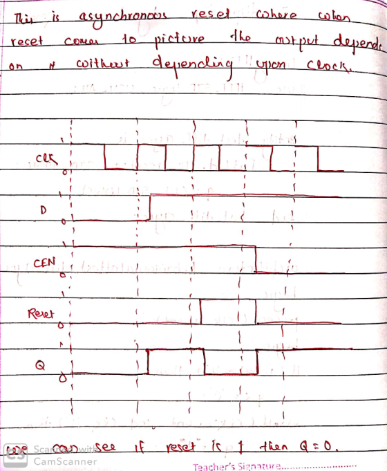
 10.21 Write a behavioral Verilog module vrDnegEc for a negative-edge-triggered D flip-flop with enable and asynchronous active-low clear. Also write a test bench that instantiates your flip-flop and exercises its operation for a comprehensive input sequence.
Lab Description Follow the instructions in the lab tasks below to behaviorially create and simulate a flip-flop. Af...
 Lab Description Follow the instructions in the lab tasks below to behaviorially create and simulate a flip-flop. Afterwards, you will create a register and use your ALU from Lab 3 to create an accumulator-based processor. This will act ike a simple processor; the ALU will execute si operations and each result will be stored in the register. In an accumulator, the value of the register will be updated with each operation; the register is used as an input to the...
how slove 4-34, 4-35, 4-36??? I dont know that! please hlep me! 306 □ CHAPTER 4/SEQUENTIAL CIRCUITS OTABLE 4-16...
 how slove 4-34, 4-35, 4-36??? I dont know that! please hlep me!
306 □ CHAPTER 4/SEQUENTIAL CIRCUITS OTABLE 4-16 State Table for Problem 4-33 Next State Input Output Present State 4-36 4-37 0 0 0 0 4-38 Design the circuit specified by Table 4-14 and use the sequence from Problen 4-31 (either yours or the one posted on the text website) to perform an automatic logic simulation-based verification of your design. 4 433. The state table for a sequential circuit...
how slove 4-34, 4-35, 4-36??? I dont know that! please hlep me!
306 □ CHAPTER 4/SEQUENTIAL CIRCUITS OTABLE 4-16 State Table for Problem 4-33 Next State Input Output Present State 4-36 4-37 0 0 0 0 4-38 Design the circuit specified by Table 4-14 and use the sequence from Problen 4-31 (either yours or the one posted on the text website) to perform an automatic logic simulation-based verification of your design. 4 433. The state table for a sequential circuit...
 a) (5 marks) Explain the difference between a latch, a gated latch and a flip flop. b) (5 marks) A gated SR latch has the following schematic diagram CLK a) Draw a timing diagram showing the Q and Q outputs for the following sequence of inputs: CLK R Assume that the initial state of the outputs is Q 0 and Q 1 c) (5 marks) Draw a schematic diagram for a rising edge-triggered master-slave D flip- flop built using two...
 10.21 Write a behavioral Verilog module vrDnegEc for a negative-edge-triggered D flip-flop with enable and asynchronous active-low clear. Also write a test bench that instantiates your flip-flop and exercises its operation for a comprehensive input sequence.
 Lab Description Follow the instructions in the lab tasks below to behaviorially create and simulate a flip-flop. Afterwards, you will create a register and use your ALU from Lab 3 to create an accumulator-based processor. This will act ike a simple processor; the ALU will execute si operations and each result will be stored in the register. In an accumulator, the value of the register will be updated with each operation; the register is used as an input to the...
 how slove 4-34, 4-35, 4-36??? I dont know that! please hlep me!
306 □ CHAPTER 4/SEQUENTIAL CIRCUITS OTABLE 4-16 State Table for Problem 4-33 Next State Input Output Present State 4-36 4-37 0 0 0 0 4-38 Design the circuit specified by Table 4-14 and use the sequence from Problen 4-31 (either yours or the one posted on the text website) to perform an automatic logic simulation-based verification of your design. 4 433. The state table for a sequential circuit...
how slove 4-34, 4-35, 4-36??? I dont know that! please hlep me!
306 □ CHAPTER 4/SEQUENTIAL CIRCUITS OTABLE 4-16 State Table for Problem 4-33 Next State Input Output Present State 4-36 4-37 0 0 0 0 4-38 Design the circuit specified by Table 4-14 and use the sequence from Problen 4-31 (either yours or the one posted on the text website) to perform an automatic logic simulation-based verification of your design. 4 433. The state table for a sequential circuit...
Most questions answered within 3 hours.
-
public enum Rating {
GENERAL(0),
PARENTALGUIDANCE(1),
MATURE(2);
asked 3 minutes ago -
A certain shop repairs both audio and video components. Let
A denote the event that the...
asked 7 minutes ago -
Modern Human Relations at the workplace- Human resource
management
Communities of practice (COPs) refers to groups...
asked 17 minutes ago -
Briefly compare and contrast Array Processors and
Multiprocessors. Mention at least two similarities and three
dissimilarities.
asked 17 minutes ago -
When looking at the unemployment rates for various countries,
which of the following is a reason...
asked 18 minutes ago -
calculate the ratio of the two iconic forms that exist in solution
for the amino acid...
asked 29 minutes ago -
1. A black hole with a larger mass will have a __________
thermal luminosity.
2. From...
asked 34 minutes ago -
Which is a criterion-referenced standard?
Someone who is accepted into graduate school.
Someone who is of...
asked 44 minutes ago -
A beaker with 1.90×10² mL of an acetic acid buffer
with a pH of 5.000 is...
asked 44 minutes ago -
define the concept of emotional labor. describe,
explain and discuss perspectives on emotional labor in general...
asked 44 minutes ago -
The unsigned decimal value (1,036)(base 10) is to be stored as a
16-bit word in memory....
asked 46 minutes ago -
(1 point) For a group of 80 people, assuming that each person is
equally likely to...
asked 1 hour ago