
Homework Answers


Add Answer to:
a) (5 marks) Explain the difference between a latch, a gated latch and a flip flop....
Use the gated SR latch design with only NAND gates to design a gated SR flip–flop....
Use the gated SR latch design with only NAND gates to design a gated SR flip–flop. The stored bit Q can only change on the positive edge (rising edge) of the clock cycle. Draw the circuit using only logic gates and create a symbol for the flip–flop you designed.
Draw waveforms for the indicated latch and flip-flop outputs. The initial value for each output is...
 Draw waveforms for the indicated latch and flip-flop outputs.
The initial value for each output is 0 as shown.
CLK D Transparent low latch Q Transparent high latch Q Negative Edge Triggered Flip-flop Q Positive Edge Triggered Flip-flop Q
Draw waveforms for the indicated latch and flip-flop outputs.
The initial value for each output is 0 as shown.
CLK D Transparent low latch Q Transparent high latch Q Negative Edge Triggered Flip-flop Q Positive Edge Triggered Flip-flop Q
Use the Quartus Prime Text Editor to implement a behavioral model of the D flip-flop described ab...
 Use the Quartus Prime Text Editor to implement a behavioral
model of the D flip-flop described above in a file named
d_flops.sv. Specify the D flip-flop’s module according to the
interface specification given in the table below.
Port
Mode
Data Type
Size
Description
RST
in
logic
1-bit
Active high asynchronous reset
CLK
in
logic
1-bit
Synchronizing clock signal
EN
in
logic
1-bit
Synchronous clock enable
D
in
logic
1-bit
Synchronous data input
Q
out
logic
1-bit
Current/present state
Qbar
out...
Use the Quartus Prime Text Editor to implement a behavioral
model of the D flip-flop described above in a file named
d_flops.sv. Specify the D flip-flop’s module according to the
interface specification given in the table below.
Port
Mode
Data Type
Size
Description
RST
in
logic
1-bit
Active high asynchronous reset
CLK
in
logic
1-bit
Synchronizing clock signal
EN
in
logic
1-bit
Synchronous clock enable
D
in
logic
1-bit
Synchronous data input
Q
out
logic
1-bit
Current/present state
Qbar
out...
QUESTION 7 A master slave flip flop behaves similarly to a clocked latch, except that the...
 QUESTION 7 A master slave flip flop behaves similarly to a clocked latch, except that the latches output can change only near the rising edge of the clock True False QUESTION 8 Assuming zero setup and hold times, clocked latches and flip-flops produce the same outputs as long as the inputs do not change while the clock is asserted True False QUESTIONS An edge-triggered D flip-flop requires more internal gates than a similar device constructed from a J-K master-slave flip...
3. Answer the following questions about a data flip-flop (D-Flip Flop): a) (4 ps) Write the VHDL required to define a rising-edge triggered (RET) D-Flip Flop with additional clock enable (CEN) an...
 3. Answer the following questions about a data flip-flop (D-Flip Flop): a) (4 ps) Write the VHDL required to define a rising-edge triggered (RET) D-Flip Flop with additional clock enable (CEN) and reset inputs. Your reset may be synchronous or asynchronous. Assume any input, output, or signal variables that you require have already been declared in VHDL (you do not have to write the declarations for these) b) [I pal ls your reset syachronous or asynchronous for the D-Flip Flop...
please answer all thanks very much! Question 3 Shown below is a schematic diagram of a...
 please answer all thanks very much!
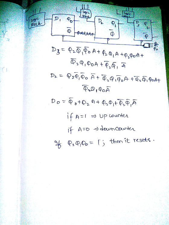
Question 3 Shown below is a schematic diagram of a counter made up of three JK flip-flops. (d) Shown below is a master-slave D flip-flop. This is made using two gated D latches. The truth table for a gated D latch is also shown below. HIGH J J CLK ас ас ac Truth table: gated D latch D EN D D, Q. D, 0. 0 0 go CLK ΕΝΟ ENO: 0 0 1 0...
please answer all thanks very much!
Question 3 Shown below is a schematic diagram of a counter made up of three JK flip-flops. (d) Shown below is a master-slave D flip-flop. This is made using two gated D latches. The truth table for a gated D latch is also shown below. HIGH J J CLK ас ас ac Truth table: gated D latch D EN D D, Q. D, 0. 0 0 go CLK ΕΝΟ ENO: 0 0 1 0...
Draw the gate level circuit schematic of a D flip-flop and a T flip-flop based on the cross-coupled NAND latch. Briefly discuss the timing behavior of a D flip-flop, a T flip-flop and a latch. (a) (8...
 Draw the gate level circuit schematic of a D flip-flop and a T flip-flop based on the cross-coupled NAND latch. Briefly discuss the timing behavior of a D flip-flop, a T flip-flop and a latch. (a) (8 Marks) circuit has three inputs, S, C and C2. S is the control input. When S-O, the circuit behaves like a D flip-flop, and when S-1, the circuit behaves like a T flip-flop. The input characteristics of the circuit are tabulated in Table...
All flip flops are positive-edge triggered. Assume each flip flop starts at 0.
 All flip flops are
positive-edge triggered. Assume each flip flop starts at 0.
Problem 11: (8 pts) For the following circuit, complete the timing diagram for the state of each flip flop and the output, where shown. All flip flops are positive-edge triggered. Assume each flip flop starts at 0. J-K FF TFF CLK PRE CLR PRE CLR CLR回 Clock CLR
Problem 11: (8 pts) For the following circuit, complete the timing diagram for the state of each flip flop...
All flip flops are
positive-edge triggered. Assume each flip flop starts at 0.
Problem 11: (8 pts) For the following circuit, complete the timing diagram for the state of each flip flop and the output, where shown. All flip flops are positive-edge triggered. Assume each flip flop starts at 0. J-K FF TFF CLK PRE CLR PRE CLR CLR回 Clock CLR
Problem 11: (8 pts) For the following circuit, complete the timing diagram for the state of each flip flop...
23. A J-K flip-flop has a l on the J input and a 0 on the...
 23. A J-K flip-flop has a l on the J input and a 0 on the K input. What state is the flip-flop in? (a) Q=1,0-0 (b) Q-1, Q-1 (c) Q-0,Q 1 (d) Q-0,Q-0 -24. On a positive edge-triggered S-R flip-flop, the outputs reflect the input condition when (a) the clock pulse is LOW (b) the clock pulse is HIGH (c) the clock pulse transitions from LOW to HIGH (d) the clock pulse transitions from HIGH to LOW 25. The...
Design a double edge-triggered D flip-flop. The output of the flip-flop Q should "sample" the value...
 Design a double edge-triggered D flip-flop. The output of the flip-flop Q should "sample" the value of the input D on both rising (+ve) and falling (-ve) edges of the clock CLK. Design an FSM counter that counts the sequence: 00, 11, 01, 10,00, 11, ..
 Draw waveforms for the indicated latch and flip-flop outputs.
The initial value for each output is 0 as shown.
CLK D Transparent low latch Q Transparent high latch Q Negative Edge Triggered Flip-flop Q Positive Edge Triggered Flip-flop Q
Draw waveforms for the indicated latch and flip-flop outputs.
The initial value for each output is 0 as shown.
CLK D Transparent low latch Q Transparent high latch Q Negative Edge Triggered Flip-flop Q Positive Edge Triggered Flip-flop Q
 Use the Quartus Prime Text Editor to implement a behavioral
model of the D flip-flop described above in a file named
d_flops.sv. Specify the D flip-flop’s module according to the
interface specification given in the table below.
Port
Mode
Data Type
Size
Description
RST
in
logic
1-bit
Active high asynchronous reset
CLK
in
logic
1-bit
Synchronizing clock signal
EN
in
logic
1-bit
Synchronous clock enable
D
in
logic
1-bit
Synchronous data input
Q
out
logic
1-bit
Current/present state
Qbar
out...
Use the Quartus Prime Text Editor to implement a behavioral
model of the D flip-flop described above in a file named
d_flops.sv. Specify the D flip-flop’s module according to the
interface specification given in the table below.
Port
Mode
Data Type
Size
Description
RST
in
logic
1-bit
Active high asynchronous reset
CLK
in
logic
1-bit
Synchronizing clock signal
EN
in
logic
1-bit
Synchronous clock enable
D
in
logic
1-bit
Synchronous data input
Q
out
logic
1-bit
Current/present state
Qbar
out...
 QUESTION 7 A master slave flip flop behaves similarly to a clocked latch, except that the latches output can change only near the rising edge of the clock True False QUESTION 8 Assuming zero setup and hold times, clocked latches and flip-flops produce the same outputs as long as the inputs do not change while the clock is asserted True False QUESTIONS An edge-triggered D flip-flop requires more internal gates than a similar device constructed from a J-K master-slave flip...
 3. Answer the following questions about a data flip-flop (D-Flip Flop): a) (4 ps) Write the VHDL required to define a rising-edge triggered (RET) D-Flip Flop with additional clock enable (CEN) and reset inputs. Your reset may be synchronous or asynchronous. Assume any input, output, or signal variables that you require have already been declared in VHDL (you do not have to write the declarations for these) b) [I pal ls your reset syachronous or asynchronous for the D-Flip Flop...
 please answer all thanks very much!
Question 3 Shown below is a schematic diagram of a counter made up of three JK flip-flops. (d) Shown below is a master-slave D flip-flop. This is made using two gated D latches. The truth table for a gated D latch is also shown below. HIGH J J CLK ас ас ac Truth table: gated D latch D EN D D, Q. D, 0. 0 0 go CLK ΕΝΟ ENO: 0 0 1 0...
please answer all thanks very much!
Question 3 Shown below is a schematic diagram of a counter made up of three JK flip-flops. (d) Shown below is a master-slave D flip-flop. This is made using two gated D latches. The truth table for a gated D latch is also shown below. HIGH J J CLK ас ас ac Truth table: gated D latch D EN D D, Q. D, 0. 0 0 go CLK ΕΝΟ ENO: 0 0 1 0...
 Draw the gate level circuit schematic of a D flip-flop and a T flip-flop based on the cross-coupled NAND latch. Briefly discuss the timing behavior of a D flip-flop, a T flip-flop and a latch. (a) (8 Marks) circuit has three inputs, S, C and C2. S is the control input. When S-O, the circuit behaves like a D flip-flop, and when S-1, the circuit behaves like a T flip-flop. The input characteristics of the circuit are tabulated in Table...
 All flip flops are
positive-edge triggered. Assume each flip flop starts at 0.
Problem 11: (8 pts) For the following circuit, complete the timing diagram for the state of each flip flop and the output, where shown. All flip flops are positive-edge triggered. Assume each flip flop starts at 0. J-K FF TFF CLK PRE CLR PRE CLR CLR回 Clock CLR
Problem 11: (8 pts) For the following circuit, complete the timing diagram for the state of each flip flop...
All flip flops are
positive-edge triggered. Assume each flip flop starts at 0.
Problem 11: (8 pts) For the following circuit, complete the timing diagram for the state of each flip flop and the output, where shown. All flip flops are positive-edge triggered. Assume each flip flop starts at 0. J-K FF TFF CLK PRE CLR PRE CLR CLR回 Clock CLR
Problem 11: (8 pts) For the following circuit, complete the timing diagram for the state of each flip flop...
 23. A J-K flip-flop has a l on the J input and a 0 on the K input. What state is the flip-flop in? (a) Q=1,0-0 (b) Q-1, Q-1 (c) Q-0,Q 1 (d) Q-0,Q-0 -24. On a positive edge-triggered S-R flip-flop, the outputs reflect the input condition when (a) the clock pulse is LOW (b) the clock pulse is HIGH (c) the clock pulse transitions from LOW to HIGH (d) the clock pulse transitions from HIGH to LOW 25. The...
 Design a double edge-triggered D flip-flop. The output of the flip-flop Q should "sample" the value of the input D on both rising (+ve) and falling (-ve) edges of the clock CLK. Design an FSM counter that counts the sequence: 00, 11, 01, 10,00, 11, ..
Most questions answered within 3 hours.
-
On April 1, 2018, Windel Corporation issued bonds with
detachable warrants.
Information related to these bonds...
asked 1 second from now -
public enum Rating {
GENERAL(0),
PARENTALGUIDANCE(1),
MATURE(2);
asked 4 minutes ago -
A certain shop repairs both audio and video components. Let
A denote the event that the...
asked 8 minutes ago -
Modern Human Relations at the workplace- Human resource
management
Communities of practice (COPs) refers to groups...
asked 18 minutes ago -
Briefly compare and contrast Array Processors and
Multiprocessors. Mention at least two similarities and three
dissimilarities.
asked 18 minutes ago -
When looking at the unemployment rates for various countries,
which of the following is a reason...
asked 19 minutes ago -
calculate the ratio of the two iconic forms that exist in solution
for the amino acid...
asked 30 minutes ago -
1. A black hole with a larger mass will have a __________
thermal luminosity.
2. From...
asked 35 minutes ago -
Which is a criterion-referenced standard?
Someone who is accepted into graduate school.
Someone who is of...
asked 45 minutes ago -
A beaker with 1.90×10² mL of an acetic acid buffer
with a pH of 5.000 is...
asked 45 minutes ago -
define the concept of emotional labor. describe,
explain and discuss perspectives on emotional labor in general...
asked 46 minutes ago -
The unsigned decimal value (1,036)(base 10) is to be stored as a
16-bit word in memory....
asked 47 minutes ago