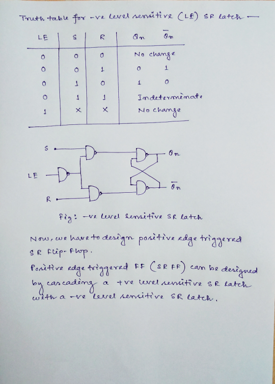
Use the gated SR latch design with only NAND gates to design a gated SR flip–flop....
Use the gated SR latch design with only NAND gates to design a gated SR flip–flop. The stored bit Q can only change on the positive edge (rising edge) of the clock cycle. Draw the circuit using only logic gates and create a symbol for the flip–flop you designed.
Homework Answers
Given problem has been solved with proper design and explanation. To understand this problem, a basic knowledge of SR Flip flop is required. If you have any doubt, please comment.
Here, level sensitive SR latches are gated SR latches.


Add Answer to:
Use the gated SR latch design with only NAND gates to design a
gated SR flip–flop....
a) (5 marks) Explain the difference between a latch, a gated latch and a flip flop....
 a) (5 marks) Explain the difference between a latch, a gated latch and a flip flop. b) (5 marks) A gated SR latch has the following schematic diagram CLK a) Draw a timing diagram showing the Q and Q outputs for the following sequence of inputs: CLK R Assume that the initial state of the outputs is Q 0 and Q 1 c) (5 marks) Draw a schematic diagram for a rising edge-triggered master-slave D flip- flop built using two...
5.4 2um 4-34. Design a negative-edge-triggered flip-flop. The flip flop has three inputs; these are Data,...
 5.4 2um
4-34. Design a negative-edge-triggered flip-flop. The flip flop has three inputs; these are Data, Clock, and Enable. If, at the negative edge of the clock, the enable input equals to 0, then the state at Data input is stored in the flip-flop. If, at the negative edge of clock, Enable is in 1 state, then the current stored value in the flip-flop is held. Design the flip-flop using only SR latches, AND gates, and NOT gates.
4-34. Design...
5.4 2um
4-34. Design a negative-edge-triggered flip-flop. The flip flop has three inputs; these are Data, Clock, and Enable. If, at the negative edge of the clock, the enable input equals to 0, then the state at Data input is stored in the flip-flop. If, at the negative edge of clock, Enable is in 1 state, then the current stored value in the flip-flop is held. Design the flip-flop using only SR latches, AND gates, and NOT gates.
4-34. Design...
a) Draw an SR-latch using only NAND gates. Label each input and output, and label all...
a) Draw an SR-latch using only NAND gates. Label each input and output, and label all wires with a name if the wire does not connect to any input or output b) Describe the behavior of the latch when S and R are both 0. What is the output of each gate? c) Assuming that the latch starts with S = R = 0, write down the sequence of what happens when R = 1. Discuss changes at each point...
a) Draw SR latch impeltation in NOR gates provied function table b) Show how D latch...
a) Draw SR latch impeltation in NOR gates provied function table b) Show how D latch (transprent) can be made from NOR gate. SR latch is transprent when it comes to storing data. c) What is limitation of D latch in terms of storing data ? what does it achive for digital terms d) Design a D flip flop that is -ve edge trigged using master slave combination of D latches designed in b) Inverters may be needed.
Design a positive-edge T flip-flop using a positive-edge-triggered D flip-flop and other logic gates.
Design a positive-edge T flip-flop using a positive-edge-triggered D flip-flop and other logic gates.
Use the Quartus Prime Text Editor to implement a behavioral model of the D flip-flop described ab...
 Use the Quartus Prime Text Editor to implement a behavioral
model of the D flip-flop described above in a file named
d_flops.sv. Specify the D flip-flop’s module according to the
interface specification given in the table below.
Port
Mode
Data Type
Size
Description
RST
in
logic
1-bit
Active high asynchronous reset
CLK
in
logic
1-bit
Synchronizing clock signal
EN
in
logic
1-bit
Synchronous clock enable
D
in
logic
1-bit
Synchronous data input
Q
out
logic
1-bit
Current/present state
Qbar
out...
Use the Quartus Prime Text Editor to implement a behavioral
model of the D flip-flop described above in a file named
d_flops.sv. Specify the D flip-flop’s module according to the
interface specification given in the table below.
Port
Mode
Data Type
Size
Description
RST
in
logic
1-bit
Active high asynchronous reset
CLK
in
logic
1-bit
Synchronizing clock signal
EN
in
logic
1-bit
Synchronous clock enable
D
in
logic
1-bit
Synchronous data input
Q
out
logic
1-bit
Current/present state
Qbar
out...
Draw the gate level circuit schematic of a D flip-flop and a T flip-flop based on the cross-coupled NAND latch. Briefly discuss the timing behavior of a D flip-flop, a T flip-flop and a latch. (a) (8...
 Draw the gate level circuit schematic of a D flip-flop and a T flip-flop based on the cross-coupled NAND latch. Briefly discuss the timing behavior of a D flip-flop, a T flip-flop and a latch. (a) (8 Marks) circuit has three inputs, S, C and C2. S is the control input. When S-O, the circuit behaves like a D flip-flop, and when S-1, the circuit behaves like a T flip-flop. The input characteristics of the circuit are tabulated in Table...
Provide a complementary CMOS transistor circuit design for a a) NOR based SR flip-flop b) NAND...
 Provide a complementary CMOS transistor circuit design for a a) NOR based SR flip-flop b) NAND based SR flip-flop
QUESTION 7 A master slave flip flop behaves similarly to a clocked latch, except that the...
 QUESTION 7 A master slave flip flop behaves similarly to a clocked latch, except that the latches output can change only near the rising edge of the clock True False QUESTION 8 Assuming zero setup and hold times, clocked latches and flip-flops produce the same outputs as long as the inputs do not change while the clock is asserted True False QUESTIONS An edge-triggered D flip-flop requires more internal gates than a similar device constructed from a J-K master-slave flip...
9. (15 points) The D latch shown in lecture 15 slide 15 is constructed with four NAND gates and a...
 9. (15 points) The D latch shown in lecture 15 slide 15 is constructed with four NAND gates and an inverter. Consider the following three other ways for obtaining a D latch, and in each case draw the logic diagram and verify the circuit operation Use NOR gates for the SR latch part and AND gates for the other two. An inverter may be needed. Use NOR gates for all four gates. Inverters may be needed. i. ii. Use four...
 a) (5 marks) Explain the difference between a latch, a gated latch and a flip flop. b) (5 marks) A gated SR latch has the following schematic diagram CLK a) Draw a timing diagram showing the Q and Q outputs for the following sequence of inputs: CLK R Assume that the initial state of the outputs is Q 0 and Q 1 c) (5 marks) Draw a schematic diagram for a rising edge-triggered master-slave D flip- flop built using two...
 5.4 2um
4-34. Design a negative-edge-triggered flip-flop. The flip flop has three inputs; these are Data, Clock, and Enable. If, at the negative edge of the clock, the enable input equals to 0, then the state at Data input is stored in the flip-flop. If, at the negative edge of clock, Enable is in 1 state, then the current stored value in the flip-flop is held. Design the flip-flop using only SR latches, AND gates, and NOT gates.
4-34. Design...
5.4 2um
4-34. Design a negative-edge-triggered flip-flop. The flip flop has three inputs; these are Data, Clock, and Enable. If, at the negative edge of the clock, the enable input equals to 0, then the state at Data input is stored in the flip-flop. If, at the negative edge of clock, Enable is in 1 state, then the current stored value in the flip-flop is held. Design the flip-flop using only SR latches, AND gates, and NOT gates.
4-34. Design...
 Use the Quartus Prime Text Editor to implement a behavioral
model of the D flip-flop described above in a file named
d_flops.sv. Specify the D flip-flop’s module according to the
interface specification given in the table below.
Port
Mode
Data Type
Size
Description
RST
in
logic
1-bit
Active high asynchronous reset
CLK
in
logic
1-bit
Synchronizing clock signal
EN
in
logic
1-bit
Synchronous clock enable
D
in
logic
1-bit
Synchronous data input
Q
out
logic
1-bit
Current/present state
Qbar
out...
Use the Quartus Prime Text Editor to implement a behavioral
model of the D flip-flop described above in a file named
d_flops.sv. Specify the D flip-flop’s module according to the
interface specification given in the table below.
Port
Mode
Data Type
Size
Description
RST
in
logic
1-bit
Active high asynchronous reset
CLK
in
logic
1-bit
Synchronizing clock signal
EN
in
logic
1-bit
Synchronous clock enable
D
in
logic
1-bit
Synchronous data input
Q
out
logic
1-bit
Current/present state
Qbar
out...
 Draw the gate level circuit schematic of a D flip-flop and a T flip-flop based on the cross-coupled NAND latch. Briefly discuss the timing behavior of a D flip-flop, a T flip-flop and a latch. (a) (8 Marks) circuit has three inputs, S, C and C2. S is the control input. When S-O, the circuit behaves like a D flip-flop, and when S-1, the circuit behaves like a T flip-flop. The input characteristics of the circuit are tabulated in Table...
 Provide a complementary CMOS transistor circuit design for a a) NOR based SR flip-flop b) NAND based SR flip-flop
 QUESTION 7 A master slave flip flop behaves similarly to a clocked latch, except that the latches output can change only near the rising edge of the clock True False QUESTION 8 Assuming zero setup and hold times, clocked latches and flip-flops produce the same outputs as long as the inputs do not change while the clock is asserted True False QUESTIONS An edge-triggered D flip-flop requires more internal gates than a similar device constructed from a J-K master-slave flip...
 9. (15 points) The D latch shown in lecture 15 slide 15 is constructed with four NAND gates and an inverter. Consider the following three other ways for obtaining a D latch, and in each case draw the logic diagram and verify the circuit operation Use NOR gates for the SR latch part and AND gates for the other two. An inverter may be needed. Use NOR gates for all four gates. Inverters may be needed. i. ii. Use four...
Most questions answered within 3 hours.
-
> Women’s pulse rates are normally distributed with a mean of
68.5 beats per minute and...
asked 1 minute ago -
Briefly describe an aspect of the strengths perspective that is
consistent with your own understanding of...
asked 2 minutes ago -
Step by step method of using Sparse Identification of Nonlinear
Dynamics (SINDy) to model your own...
asked 10 minutes ago -
3) What are the typical social structures in a global city?
asked 3 hours ago -
Luther Corporation
Consolidated Balance Sheet
December 31, 2019 and 2018 (in $ millions)
Assets
2019
2018...
asked 3 hours ago -
(Expected rate of return and risk) Carter Inc. is evaluating a
security. Calculate the investment’s expected...
asked 6 hours ago -
What specific indicators can point to lack of progress for
African Americans in American society?
asked 7 hours ago -
1-The Electrons in a beam are moving at 2.7×10⁸ m/s in an
electric field of 15000...
asked 7 hours ago -
A gas tank is a vertical cylinder. It has a radius of 1m, a
height of...
asked 7 hours ago -
Accent Software faces the following conditions. All of these
support Accent’s use of a market-penetration pricing...
asked 8 hours ago -
A mathematically inclined friend emails you the following
instructions: "Meet me in the cafeteria the first...
asked 8 hours ago -
A monopoly sells in two countries . The demand curves in the two
countries are p1...
asked 9 hours ago