
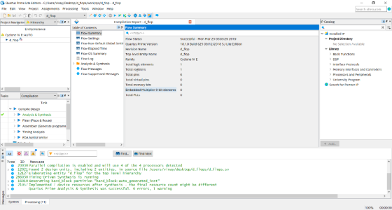
Use the Quartus Prime Text Editor to implement a behavioral model of the D flip-flop described above in a file named d_flops.sv. Specify the D flip-flop’s module according to the interface specification given in the table below.
|
Port |
Mode |
Data Type |
Size |
Description |
|
RST |
in |
logic |
1-bit |
Active high asynchronous reset |
|
CLK |
in |
logic |
1-bit |
Synchronizing clock signal |
|
EN |
in |
logic |
1-bit |
Synchronous clock enable |
|
D |
in |
logic |
1-bit |
Synchronous data input |
|
Q |
out |
logic |
1-bit |
Current/present state |
|
Qbar |
out |
logic |
1-bit |
Inverted current/present state |
Within the module implementation, model the D flip-flop using the following modeling specifications:
-
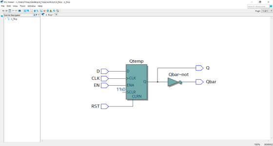
Declare an intermediate signal named Qtemp of type logic. Signal Qtemprepresents the current state of the D flip-flop.
-
Utilize a concurrent sensitivity-list always_ff @ ( ) statement to represent the behavior of the D flip flop. Which signal(s) should be included in the sensitivity list?(Don’t forget to enclose this in a begin – end block if needed)
-
Within the sensitivity list, detect the rising edge of port signals CLK and RST using the keyword posedge. See the example below:
always_ff @(posedge name_signal)
-
Within the implementation portion of the always @ statement, use nestedsequential if statements to model the behavior of the D flip-flop. What signal(s), if any, have priority? (Don’t forget to enclose this in a begin – end block if needed)
-
Properly assign port signals Q and Qbar.
Homework Answers
//D Flip Flop in SV
module d_flop(
input logic RST,CLK,EN,D, //Input port Declaration
output logic Q,Qbar //Output port Declaration
);
logic Qtemp; //Internal Variable
//Sequential BLOCK using nested if
always_ff @(posedge CLK or posedge RST) begin
if(RST) //Set = 1 or posedge of RST
Qtemp <= 1'b0;
else if(EN) //EN = 1
Qtemp <= D;
else //EN = 0, HOLD previous value
Qtemp <= Qtemp;
end
//Assigning Output Ports
assign Q = Qtemp;
assign Qbar = ~Qtemp;
endmodule
//Testbench in SV
module test;
logic RST,CLK,EN,D,Q,Qbar;
//Instantiation of D Flip Flop
d_flop DFF(RST,CLK,EN,D,Q,Qbar);
//Driving Clock
always begin
#5 CLK = 1'b0;
#5 CLK = ~CLK;
end
//Driving Stimulus
initial begin
RST = 1'b1;
@(posedge CLK) RST = 1'b0;
EN = 0; D = 0;
@(posedge CLK) EN = 0; D = 1;
@(posedge CLK) EN = 1; D = 1;
@(posedge CLK) EN = 1; D = 0;
@(posedge CLK) EN = 1; D = 1;
@(posedge CLK) EN = 0; D = 0;
@(posedge CLK) EN = 1; D = 1;
@(posedge CLK) $finish;s
end
endmodule
//Simulation Waveform

//Quartus Synthesis
Add Answer to:
Use the Quartus Prime Text Editor to implement a behavioral model of the D flip-flop described ab...
Use the Quartus Prime Text Editor to implement a structural model of the 4-bit data register show...
 Use the Quartus Prime Text Editor to implement a structural
model of the 4-bit data register shown above in a file named
reg_4bit.sv. Specify the 4-bit data register’s module according to
the interface specification given in the table below.
Port
Mode
Data Type
Size
Description
RST
in
logic
1-bit
Active high asynchronous reset
CLK
in
logic
1-bit
Synchronizing clock signal
EN
in
logic
1-bit
Synchronous clock enable
D
in
logic vector
4-bits
Synchronous data input
Q
out
logic vector
4-bits...
Use the Quartus Prime Text Editor to implement a structural
model of the 4-bit data register shown above in a file named
reg_4bit.sv. Specify the 4-bit data register’s module according to
the interface specification given in the table below.
Port
Mode
Data Type
Size
Description
RST
in
logic
1-bit
Active high asynchronous reset
CLK
in
logic
1-bit
Synchronizing clock signal
EN
in
logic
1-bit
Synchronous clock enable
D
in
logic vector
4-bits
Synchronous data input
Q
out
logic vector
4-bits...
a) (5 marks) Explain the difference between a latch, a gated latch and a flip flop....
 a) (5 marks) Explain the difference between a latch, a gated latch and a flip flop. b) (5 marks) A gated SR latch has the following schematic diagram CLK a) Draw a timing diagram showing the Q and Q outputs for the following sequence of inputs: CLK R Assume that the initial state of the outputs is Q 0 and Q 1 c) (5 marks) Draw a schematic diagram for a rising edge-triggered master-slave D flip- flop built using two...
3. Answer the following questions about a data flip-flop (D-Flip Flop): a) (4 ps) Write the VHDL required to define a rising-edge triggered (RET) D-Flip Flop with additional clock enable (CEN) an...
 3. Answer the following questions about a data flip-flop (D-Flip Flop): a) (4 ps) Write the VHDL required to define a rising-edge triggered (RET) D-Flip Flop with additional clock enable (CEN) and reset inputs. Your reset may be synchronous or asynchronous. Assume any input, output, or signal variables that you require have already been declared in VHDL (you do not have to write the declarations for these) b) [I pal ls your reset syachronous or asynchronous for the D-Flip Flop...
1. a) Complete the waveform templates for the Master –Slave D-flip-flop below with given D, CLK,...
 1.
a) Complete the waveform templates for the Master –Slave
D-flip-flop below with given D, CLK, CLEAR, and PRESET signals.
Neglect the propagation delays.
b) Does it have positive or negative edge triggering with
respect to CLK?
c) Are the asynchronous PRESET and CLEAR active-high or
active-low?
2. Enabling of data load in the D-flip-flop was implemented with
a 2-to-1 multiplexer as show below. The D-flip-flop has the
positive edge triggering and the active-low asynchronous clear.
a) Is the Enable...
1.
a) Complete the waveform templates for the Master –Slave
D-flip-flop below with given D, CLK, CLEAR, and PRESET signals.
Neglect the propagation delays.
b) Does it have positive or negative edge triggering with
respect to CLK?
c) Are the asynchronous PRESET and CLEAR active-high or
active-low?
2. Enabling of data load in the D-flip-flop was implemented with
a 2-to-1 multiplexer as show below. The D-flip-flop has the
positive edge triggering and the active-low asynchronous clear.
a) Is the Enable...
1. The D Flip-Flop ) Look for the datasheet of the 7474 D flip-flop and wire it on the breadboard...
 1. The D Flip-Flop ) Look for the datasheet of the 7474 D flip-flop and wire it on the breadboard making sure to supply 5V to both Preset and Clear. Utilize the function generator to provide a Clock signal of 1 Hz: i) Press AMPL and set value to 5 Vpp ii) Press FREQ and set value to 1 Hz ili) Press OFFSET and set value to 2.5 V This Clock signal will be the same for all circuits in...
23. A J-K flip-flop has a l on the J input and a 0 on the...
 23. A J-K flip-flop has a l on the J input and a 0 on the K input. What state is the flip-flop in? (a) Q=1,0-0 (b) Q-1, Q-1 (c) Q-0,Q 1 (d) Q-0,Q-0 -24. On a positive edge-triggered S-R flip-flop, the outputs reflect the input condition when (a) the clock pulse is LOW (b) the clock pulse is HIGH (c) the clock pulse transitions from LOW to HIGH (d) the clock pulse transitions from HIGH to LOW 25. The...
Consider the circuit in Figure 1. It is a 4-bit (QQ2Q3) synchronous counter which uses four T-typ...
 Consider the circuit in Figure 1. It is a 4-bit (QQ2Q3) synchronous counter which uses four T-type flip-flops. The counter increases its value on each positive edge of the clock if the Enable signal is asserted. The counter is reset to 0 by setting the Clear signal low. You are to implement an 8-bit counter of this type Enable T Q Clock Clear Figure 1. 4-bit synchronous counter (but you need to implement 8-bit counter in this lab) Specific notes:...
We have designed a 2NAND and 3NAND. 1. Use the cells you have already constructed to...
 We have designed a 2NAND and 3NAND.
1. Use the cells you have already constructed to design a latech, and use two latches to build a CMOS D flip-flop schematic in Cadence. Assume the flip-flop is clocked, and that clock, iclock synchronous load and synchronous load are inputs to your design. You must include asynchronous reset signals in your circuit. Load is active iugh. The flip-flop should be positive edge triggered. The clock signal should not be gated (in other...
We have designed a 2NAND and 3NAND.
1. Use the cells you have already constructed to design a latech, and use two latches to build a CMOS D flip-flop schematic in Cadence. Assume the flip-flop is clocked, and that clock, iclock synchronous load and synchronous load are inputs to your design. You must include asynchronous reset signals in your circuit. Load is active iugh. The flip-flop should be positive edge triggered. The clock signal should not be gated (in other...
Lab Description Follow the instructions in the lab tasks below to behaviorially create and simulate a flip-flop. Af...
 Lab Description Follow the instructions in the lab tasks below to behaviorially create and simulate a flip-flop. Afterwards, you will create a register and use your ALU from Lab 3 to create an accumulator-based processor. This will act ike a simple processor; the ALU will execute si operations and each result will be stored in the register. In an accumulator, the value of the register will be updated with each operation; the register is used as an input to the...
Use a behavioral Verilog model to design a 3-bit fault tolerant up-down counter. For each flip-fl...
 Use a behavioral Verilog model to design a 3-bit fault tolerant up-down counter. For each flip-flop (FF) include asynchronous reset and preset signals. Refer to Example 4.3 on page 160 for an example of a single FF with both reset and preset signals as well as with an enable signal. For this project, you don't need to use FFs with enables. You don't also need not-q (nq) in this assignment. Use active-high signals for reset and present signals. The example...
 Use the Quartus Prime Text Editor to implement a structural
model of the 4-bit data register shown above in a file named
reg_4bit.sv. Specify the 4-bit data register’s module according to
the interface specification given in the table below.
Port
Mode
Data Type
Size
Description
RST
in
logic
1-bit
Active high asynchronous reset
CLK
in
logic
1-bit
Synchronizing clock signal
EN
in
logic
1-bit
Synchronous clock enable
D
in
logic vector
4-bits
Synchronous data input
Q
out
logic vector
4-bits...
Use the Quartus Prime Text Editor to implement a structural
model of the 4-bit data register shown above in a file named
reg_4bit.sv. Specify the 4-bit data register’s module according to
the interface specification given in the table below.
Port
Mode
Data Type
Size
Description
RST
in
logic
1-bit
Active high asynchronous reset
CLK
in
logic
1-bit
Synchronizing clock signal
EN
in
logic
1-bit
Synchronous clock enable
D
in
logic vector
4-bits
Synchronous data input
Q
out
logic vector
4-bits...
 a) (5 marks) Explain the difference between a latch, a gated latch and a flip flop. b) (5 marks) A gated SR latch has the following schematic diagram CLK a) Draw a timing diagram showing the Q and Q outputs for the following sequence of inputs: CLK R Assume that the initial state of the outputs is Q 0 and Q 1 c) (5 marks) Draw a schematic diagram for a rising edge-triggered master-slave D flip- flop built using two...
 3. Answer the following questions about a data flip-flop (D-Flip Flop): a) (4 ps) Write the VHDL required to define a rising-edge triggered (RET) D-Flip Flop with additional clock enable (CEN) and reset inputs. Your reset may be synchronous or asynchronous. Assume any input, output, or signal variables that you require have already been declared in VHDL (you do not have to write the declarations for these) b) [I pal ls your reset syachronous or asynchronous for the D-Flip Flop...
 1.
a) Complete the waveform templates for the Master –Slave
D-flip-flop below with given D, CLK, CLEAR, and PRESET signals.
Neglect the propagation delays.
b) Does it have positive or negative edge triggering with
respect to CLK?
c) Are the asynchronous PRESET and CLEAR active-high or
active-low?
2. Enabling of data load in the D-flip-flop was implemented with
a 2-to-1 multiplexer as show below. The D-flip-flop has the
positive edge triggering and the active-low asynchronous clear.
a) Is the Enable...
1.
a) Complete the waveform templates for the Master –Slave
D-flip-flop below with given D, CLK, CLEAR, and PRESET signals.
Neglect the propagation delays.
b) Does it have positive or negative edge triggering with
respect to CLK?
c) Are the asynchronous PRESET and CLEAR active-high or
active-low?
2. Enabling of data load in the D-flip-flop was implemented with
a 2-to-1 multiplexer as show below. The D-flip-flop has the
positive edge triggering and the active-low asynchronous clear.
a) Is the Enable...
 1. The D Flip-Flop ) Look for the datasheet of the 7474 D flip-flop and wire it on the breadboard making sure to supply 5V to both Preset and Clear. Utilize the function generator to provide a Clock signal of 1 Hz: i) Press AMPL and set value to 5 Vpp ii) Press FREQ and set value to 1 Hz ili) Press OFFSET and set value to 2.5 V This Clock signal will be the same for all circuits in...
 23. A J-K flip-flop has a l on the J input and a 0 on the K input. What state is the flip-flop in? (a) Q=1,0-0 (b) Q-1, Q-1 (c) Q-0,Q 1 (d) Q-0,Q-0 -24. On a positive edge-triggered S-R flip-flop, the outputs reflect the input condition when (a) the clock pulse is LOW (b) the clock pulse is HIGH (c) the clock pulse transitions from LOW to HIGH (d) the clock pulse transitions from HIGH to LOW 25. The...
 Consider the circuit in Figure 1. It is a 4-bit (QQ2Q3) synchronous counter which uses four T-type flip-flops. The counter increases its value on each positive edge of the clock if the Enable signal is asserted. The counter is reset to 0 by setting the Clear signal low. You are to implement an 8-bit counter of this type Enable T Q Clock Clear Figure 1. 4-bit synchronous counter (but you need to implement 8-bit counter in this lab) Specific notes:...
 We have designed a 2NAND and 3NAND.
1. Use the cells you have already constructed to design a latech, and use two latches to build a CMOS D flip-flop schematic in Cadence. Assume the flip-flop is clocked, and that clock, iclock synchronous load and synchronous load are inputs to your design. You must include asynchronous reset signals in your circuit. Load is active iugh. The flip-flop should be positive edge triggered. The clock signal should not be gated (in other...
We have designed a 2NAND and 3NAND.
1. Use the cells you have already constructed to design a latech, and use two latches to build a CMOS D flip-flop schematic in Cadence. Assume the flip-flop is clocked, and that clock, iclock synchronous load and synchronous load are inputs to your design. You must include asynchronous reset signals in your circuit. Load is active iugh. The flip-flop should be positive edge triggered. The clock signal should not be gated (in other...
 Lab Description Follow the instructions in the lab tasks below to behaviorially create and simulate a flip-flop. Afterwards, you will create a register and use your ALU from Lab 3 to create an accumulator-based processor. This will act ike a simple processor; the ALU will execute si operations and each result will be stored in the register. In an accumulator, the value of the register will be updated with each operation; the register is used as an input to the...
 Use a behavioral Verilog model to design a 3-bit fault tolerant up-down counter. For each flip-flop (FF) include asynchronous reset and preset signals. Refer to Example 4.3 on page 160 for an example of a single FF with both reset and preset signals as well as with an enable signal. For this project, you don't need to use FFs with enables. You don't also need not-q (nq) in this assignment. Use active-high signals for reset and present signals. The example...
Most questions answered within 3 hours.
-
3) What are the typical social structures in a global city?
asked 32 minutes ago -
Luther Corporation
Consolidated Balance Sheet
December 31, 2019 and 2018 (in $ millions)
Assets
2019
2018...
asked 34 minutes ago -
(Expected rate of return and risk) Carter Inc. is evaluating a
security. Calculate the investment’s expected...
asked 3 hours ago -
What specific indicators can point to lack of progress for
African Americans in American society?
asked 4 hours ago -
1-The Electrons in a beam are moving at 2.7×10⁸ m/s in an
electric field of 15000...
asked 4 hours ago -
A gas tank is a vertical cylinder. It has a radius of 1m, a
height of...
asked 4 hours ago -
Accent Software faces the following conditions. All of these
support Accent’s use of a market-penetration pricing...
asked 5 hours ago -
A mathematically inclined friend emails you the following
instructions: "Meet me in the cafeteria the first...
asked 5 hours ago -
A monopoly sells in two countries . The demand curves in the two
countries are p1...
asked 6 hours ago -
A .15kg rubber ball is bounced off a wall. Before hitting the
wall, the ball moves...
asked 7 hours ago -
A manufacturing company preparing to build a new plant is
considering three potential locations for it....
asked 7 hours ago -
B. If compound Y has approximately the same values of solubility
in toluene as compound X,...
asked 8 hours ago