
Use the Quartus Prime Text Editor to implement a structural model of the 4-bit data register shown above in a file named reg_4bit.sv. Specify the 4-bit data register’s module according to the interface specification given in the table below.
|
Port |
Mode |
Data Type |
Size |
Description |
|
RST |
in |
logic |
1-bit |
Active high asynchronous reset |
|
CLK |
in |
logic |
1-bit |
Synchronizing clock signal |
|
EN |
in |
logic |
1-bit |
Synchronous clock enable |
|
D |
in |
logic vector |
4-bits |
Synchronous data input |
|
Q |
out |
logic vector |
4-bits |
Current/present state (data) stored by the register. |
|
Qbar |
out |
logic vector |
4-bits |
Inverted current/present state (data) stored by the register. |
Within the declaration portion of the module, perform the following declarations:
Declare a constant named REG_WIDTH (using ALL CAPS) of type integer and assign it to 4. See the example shown below.
localparam REG_WIDTH = 4;
Within the implementation portion of the module, model the parallel-in, parallel-out data register according to the following modeling specifications:
• Use a concurrent for-generate statement with the following attributes:o AgeneratelabelnamedFF_stages
-
A generate parameter named k
-
A range that includes constant REG_WIDTH and a down to direction.
o A generate body that uses a concurrent module instantiationstatement to instantiate the D flip-flops. Use an instance label named FFand associate the ports of the instances using named association.
Homework Answers
// RTL code in System verilog
//D Flip Flop in SV
module d_flop(
input logic RST,CLK,EN,D, //Input port Declaration
output logic Q,Qbar //Output port Declaration
);
logic Qtemp; //Internal Variable
//Sequential BLOCK using nested if
always_ff @(posedge CLK or posedge RST) begin
if(RST) //Set = 1 or posedge of RST
Qtemp <= 1'b0;
else if(EN) //EN = 1
Qtemp <= D;
else //EN = 0, HOLD previous value
Qtemp <= Qtemp;
end
//Assigning Output Ports
assign Q = Qtemp;
assign Qbar = ~Qtemp;
endmodule
//Data Register code in SV
module data_register(RST,CLK,EN,D,Q,Qbar);
localparam REG_WIDTH = 4;
input logic RST,CLK,EN; //Input port Declaration
input logic [REG_WIDTH-1:0]D; //Data Input port Declaration
output logic [REG_WIDTH-1:0]Q,Qbar; //Output port Declaration
// D flip flop Instantiation using generate loop based on local parameter
generate
genvar k;
for(k=0 ; k<REG_WIDTH ; k++)
begin : DFF_Instance
d_flop DFF(RST,CLK,EN,D[k],Q[k],Qbar[k]);
end
endgenerate
endmodule
//Testbench in SV
module test;
logic RST,CLK,EN;
logic [3:0]D,Q,Qbar;
//Instantiation of Data Register
data_register DATA_REGISTER(RST,CLK,EN,D,Q,Qbar);
//Driving Clock
always begin
#5 CLK = 1'b0;
#5 CLK = ~CLK;
end
//Driving Stimulus
initial begin
RST = 1'b1;
@(posedge CLK) RST = 1'b0;
EN = 0; D = 0;
@(posedge CLK) EN = 0; D = 9;
@(posedge CLK) EN = 1; D = 10;
@(posedge CLK) EN = 1; D = 0;
@(posedge CLK) EN = 1; D = 15;
@(posedge CLK) EN = 0; D = 0;
@(posedge CLK) EN = 1; D = 9;
@(posedge CLK) EN = 0;
@(posedge CLK) $finish;
end
endmodule
//Simulation Waveform

// QUARTUS synthesis
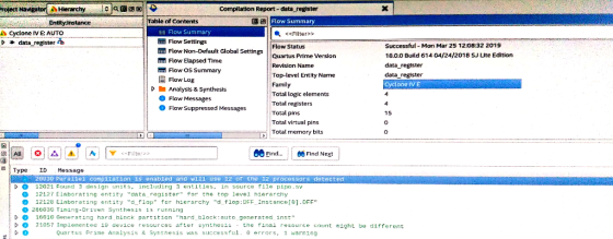
// RTL SCHEMATIC OBTAINED FROM QUARTUS SYNTHESIS
![d ropsiorr instanceloj.DrFi CLK CLU 0 Qbar Obar3.0] D 에 EN RST d flop.DFF instancel1].DFF CLK Obar EN d flop:DFF Instance 2].](http://img.homeworklib.com/images/17f1bc87-9960-49be-a16a-c4b9bd3211d5.png?x-oss-process=image/resize,w_560)
Add Answer to:
Use the Quartus Prime Text Editor to implement a structural model of the 4-bit data register show...
Use the Quartus Prime Text Editor to implement a behavioral model of the D flip-flop described ab...
 Use the Quartus Prime Text Editor to implement a behavioral
model of the D flip-flop described above in a file named
d_flops.sv. Specify the D flip-flop’s module according to the
interface specification given in the table below.
Port
Mode
Data Type
Size
Description
RST
in
logic
1-bit
Active high asynchronous reset
CLK
in
logic
1-bit
Synchronizing clock signal
EN
in
logic
1-bit
Synchronous clock enable
D
in
logic
1-bit
Synchronous data input
Q
out
logic
1-bit
Current/present state
Qbar
out...
Use the Quartus Prime Text Editor to implement a behavioral
model of the D flip-flop described above in a file named
d_flops.sv. Specify the D flip-flop’s module according to the
interface specification given in the table below.
Port
Mode
Data Type
Size
Description
RST
in
logic
1-bit
Active high asynchronous reset
CLK
in
logic
1-bit
Synchronizing clock signal
EN
in
logic
1-bit
Synchronous clock enable
D
in
logic
1-bit
Synchronous data input
Q
out
logic
1-bit
Current/present state
Qbar
out...
in VHDL Show synthesizable VHDL code for a register unit that performs operations shown below. The unit has a 3-bit mod...
 in VHDL
Show synthesizable VHDL code for a register unit that performs operations shown below. The unit has a 3-bit mode (md) input, an asynchronous reset (rs) input, a 1-bit output control (oc) input, and an 8-bit bi-directional io bus. The internal register drives the io bus when oc is ‘I, and md is not “11 1". Use std-logic. md-000: does nothing md-001: right shift the register md-010: left shift the register md 011: up count, binary md-100: down count,...
in VHDL
Show synthesizable VHDL code for a register unit that performs operations shown below. The unit has a 3-bit mode (md) input, an asynchronous reset (rs) input, a 1-bit output control (oc) input, and an 8-bit bi-directional io bus. The internal register drives the io bus when oc is ‘I, and md is not “11 1". Use std-logic. md-000: does nothing md-001: right shift the register md-010: left shift the register md 011: up count, binary md-100: down count,...
Consider the circuit in Figure 1. It is a 4-bit (QQ2Q3) synchronous counter which uses four T-typ...
 Consider the circuit in Figure 1. It is a 4-bit (QQ2Q3) synchronous counter which uses four T-type flip-flops. The counter increases its value on each positive edge of the clock if the Enable signal is asserted. The counter is reset to 0 by setting the Clear signal low. You are to implement an 8-bit counter of this type Enable T Q Clock Clear Figure 1. 4-bit synchronous counter (but you need to implement 8-bit counter in this lab) Specific notes:...
How do I change these modules so that the communication is bidirectional (inout)? I'm simply not ...
How do I change these modules so that the communication is bidirectional (inout)? I'm simply not sure how to modify the code. I know i need to add an inout port but I don't know how to do it. I have watched multiple tutorials but I can't figure it out. module mem( input logic clk, we , // write enable bit, active low input logic [n-1:0] in , input logic [m-1:0] addr , output logic [n-1:0] out ) ; parameter...
How do I change these modules so that the communication is bidirectional (inout)? I'm simply not...
How do I change these modules so that the communication is bidirectional (inout)? I'm simply not sure how to modify the code. I know i need to add an inout port but I don't know how to do it. I have watched multiple tutorials but I can't figure it out. module mem( input logic clk, we , // write enable bit, active low input logic [n-1:0] in , input logic [m-1:0] addr , output logic [n-1:0] out ) ; parameter...
Use a behavioral Verilog model to design a 3-bit fault tolerant up-down counter. For each flip-fl...
 Use a behavioral Verilog model to design a 3-bit fault tolerant up-down counter. For each flip-flop (FF) include asynchronous reset and preset signals. Refer to Example 4.3 on page 160 for an example of a single FF with both reset and preset signals as well as with an enable signal. For this project, you don't need to use FFs with enables. You don't also need not-q (nq) in this assignment. Use active-high signals for reset and present signals. The example...
Design a 3- bit Multipurpose Register. The register utilizes 3 "D" type flip flops with outputs...
Design a 3- bit Multipurpose Register. The register utilizes 3 "D" type flip flops with outputs Q0, Q1, Q2. The Registers has a synchronous clock input(CLK) that clocks all 3 flip flops on its positive edge The Registers has an asynchronous clear input(CLR' ) that sets all flip flops to "0" when active low. The Register has 2 select inputs, S0 and S1 that selects the functions as folows: S1 = 0, 0, 1, 1 and S0 = 0,1,0,1 and...
2. A 4-bit parallel in/serial out shift register has SHIFT/LOAD' and CLK inputs as shown in...
 2. A 4-bit parallel in/serial out shift register has SHIFT/LOAD' and CLK inputs as shown in the figure below. What is the output Q3 at the two times('A' followed by 'B') indicated by the dashed lines in the figure below if the parallel data inputs are DO-1, D1-0, D2-1, and D3-1? D3 SHIFT/L CLK SHIFT /LOAD Ο A. A-0,9:0 B. A:0, B-1 D.A-1, B-1
Problem 7. Consider the 74x194 4-bit bidirectional universal shift register shown below Determine the operation of...
 Problem 7. Consider the 74x194 4-bit bidirectional universal shift register shown below Determine the operation of this circuit by filling out the table. Assume that the register is cleared initially as indicated by the first row in the table, and then connected to +5V (before time t), as shown in schematic. Also assume that t 'is that time at which a positive edge occurs in the input signal 'clock'. Si and S0 inputs (given) are used to switch between modes...
17. The 74195 in Figure 17 is a synchronous load, 4-bit parallel-access shift register. For this exercise, the input data is loaded at the first active clock edge. (12 pts) 74195 DSTM2 SH/LD QB 1...
 17. The 74195 in Figure 17 is a synchronous load, 4-bit parallel-access shift register. For this exercise, the input data is loaded at the first active clock edge. (12 pts) 74195 DSTM2 SH/LD QB 13 QC QD DSTMI 10t CLK ㅡㅡㅡ CLR Figure 17 Use the circuit of Figure 17 to answer the following questions: a. Is this a ring counter or a Johnson counter? (2 pts) b. How many different states are available? (2 pts) Draw the timing diagram...
 Use the Quartus Prime Text Editor to implement a behavioral
model of the D flip-flop described above in a file named
d_flops.sv. Specify the D flip-flop’s module according to the
interface specification given in the table below.
Port
Mode
Data Type
Size
Description
RST
in
logic
1-bit
Active high asynchronous reset
CLK
in
logic
1-bit
Synchronizing clock signal
EN
in
logic
1-bit
Synchronous clock enable
D
in
logic
1-bit
Synchronous data input
Q
out
logic
1-bit
Current/present state
Qbar
out...
Use the Quartus Prime Text Editor to implement a behavioral
model of the D flip-flop described above in a file named
d_flops.sv. Specify the D flip-flop’s module according to the
interface specification given in the table below.
Port
Mode
Data Type
Size
Description
RST
in
logic
1-bit
Active high asynchronous reset
CLK
in
logic
1-bit
Synchronizing clock signal
EN
in
logic
1-bit
Synchronous clock enable
D
in
logic
1-bit
Synchronous data input
Q
out
logic
1-bit
Current/present state
Qbar
out...
 in VHDL
Show synthesizable VHDL code for a register unit that performs operations shown below. The unit has a 3-bit mode (md) input, an asynchronous reset (rs) input, a 1-bit output control (oc) input, and an 8-bit bi-directional io bus. The internal register drives the io bus when oc is ‘I, and md is not “11 1". Use std-logic. md-000: does nothing md-001: right shift the register md-010: left shift the register md 011: up count, binary md-100: down count,...
in VHDL
Show synthesizable VHDL code for a register unit that performs operations shown below. The unit has a 3-bit mode (md) input, an asynchronous reset (rs) input, a 1-bit output control (oc) input, and an 8-bit bi-directional io bus. The internal register drives the io bus when oc is ‘I, and md is not “11 1". Use std-logic. md-000: does nothing md-001: right shift the register md-010: left shift the register md 011: up count, binary md-100: down count,...
 Consider the circuit in Figure 1. It is a 4-bit (QQ2Q3) synchronous counter which uses four T-type flip-flops. The counter increases its value on each positive edge of the clock if the Enable signal is asserted. The counter is reset to 0 by setting the Clear signal low. You are to implement an 8-bit counter of this type Enable T Q Clock Clear Figure 1. 4-bit synchronous counter (but you need to implement 8-bit counter in this lab) Specific notes:...
 Use a behavioral Verilog model to design a 3-bit fault tolerant up-down counter. For each flip-flop (FF) include asynchronous reset and preset signals. Refer to Example 4.3 on page 160 for an example of a single FF with both reset and preset signals as well as with an enable signal. For this project, you don't need to use FFs with enables. You don't also need not-q (nq) in this assignment. Use active-high signals for reset and present signals. The example...
 2. A 4-bit parallel in/serial out shift register has SHIFT/LOAD' and CLK inputs as shown in the figure below. What is the output Q3 at the two times('A' followed by 'B') indicated by the dashed lines in the figure below if the parallel data inputs are DO-1, D1-0, D2-1, and D3-1? D3 SHIFT/L CLK SHIFT /LOAD Ο A. A-0,9:0 B. A:0, B-1 D.A-1, B-1
 Problem 7. Consider the 74x194 4-bit bidirectional universal shift register shown below Determine the operation of this circuit by filling out the table. Assume that the register is cleared initially as indicated by the first row in the table, and then connected to +5V (before time t), as shown in schematic. Also assume that t 'is that time at which a positive edge occurs in the input signal 'clock'. Si and S0 inputs (given) are used to switch between modes...
 17. The 74195 in Figure 17 is a synchronous load, 4-bit parallel-access shift register. For this exercise, the input data is loaded at the first active clock edge. (12 pts) 74195 DSTM2 SH/LD QB 13 QC QD DSTMI 10t CLK ㅡㅡㅡ CLR Figure 17 Use the circuit of Figure 17 to answer the following questions: a. Is this a ring counter or a Johnson counter? (2 pts) b. How many different states are available? (2 pts) Draw the timing diagram...
Most questions answered within 3 hours.
-
Two small plastic spheres are given positive electrical charges.
When they are a distance of 15.4...
asked 35 minutes ago -
how
does gravity affect the trajectory of projectile? what would be the
shape of the trajactory...
asked 27 minutes ago -
An acidic solution containing gold ions is
electrolyzed, producing gaseous oxygen (from water) at the anode...
asked 51 minutes ago -
Assume that the population of Mexico is 128
million and that the population increases 1.01
percentannually....
asked 1 hour ago -
Can someone please help me add appropriate descriptive
comments to each line of code in the...
asked 1 hour ago -
Romeo wishes to throw a bouquet of flowers to Juliet, who is on
a second-story balcony,...
asked 2 hours ago -
Why is QE a controversial monetary policy tool.
A. It may lead to excessive inflation.B. By...
asked 3 hours ago -
Principles of Programming midterm study guide help!
1.)
______ Which of the following would reference the...
asked 2 hours ago -
A finite potential well has depth U0 = 2.78 eV . What is the
penetration distance...
asked 3 hours ago -
1. The bus bars of a power station are in two sections A and B
separated...
asked 3 hours ago -
Fiscal policy is the deliberate manipulation of taxes and
government spending to alter GDP, employment, inflation...
asked 4 hours ago -
evaluating an expression using only one digit and + and - as
operators ....3+5-1+7-5+8
-----------------------
stack...
asked 4 hours ago