
Homework Answers
Add Answer to:
(iii Assuming that the transistor in the circuit in Figure 2 is in forward active mode...
D. For the transistor circuit shown in Figure 7, assuming that the transistor is in the...
 D. For the transistor circuit shown in Figure 7, assuming that the transistor is in the forward active mode, and B = 100 and VBE = 0.7V, calculate Base current 1B Collector current Ic (iii) Emitter current le (iv) Collector to emitter voltage Vce and (v) Voltage across the 2009 resistor v 3 80022 10 kV W VCE VBE مت + + 1 2001} 1 1
The NPN transistor in the circuit shown haes B-60 Assuming that the BJT is operating in the deep ...
 answer i-iv please
The NPN transistor in the circuit shown haes B-60 Assuming that the BJT is operating in the deep saturation mode ie. VCEsat-02y and VBE-07V ßforced-10. Question 3: 20% p-60) Assuming that the BJT is operating in the deep Rg i) Calculate collector current, Ic. (4%) ii) Calculate voltage VBB and base current,IB(6%) iii) If we keep VBB and Rc the same, i.e. at 1k2, what is the minimum value of RB to restore the transistor beta to...
answer i-iv please
The NPN transistor in the circuit shown haes B-60 Assuming that the BJT is operating in the deep saturation mode ie. VCEsat-02y and VBE-07V ßforced-10. Question 3: 20% p-60) Assuming that the BJT is operating in the deep Rg i) Calculate collector current, Ic. (4%) ii) Calculate voltage VBB and base current,IB(6%) iii) If we keep VBB and Rc the same, i.e. at 1k2, what is the minimum value of RB to restore the transistor beta to...
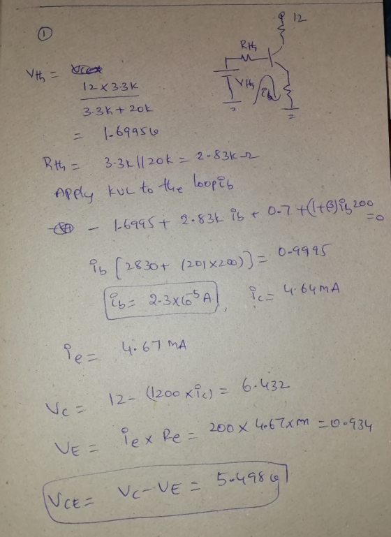
RE -3.3k2 Figure 5. Vbe-0.7V (active), Vce 0.2V (saturation), p-100 For the circuit shown in Figure...
 RE -3.3k2 Figure 5. Vbe-0.7V (active), Vce 0.2V (saturation), p-100 For the circuit shown in Figure 5: a) If V oV DC, find the DC bias point for Q1? b) Draw the small signal equivalent circuit and evaluate the small signal AC voltage gain. c) Sketch le vs Vce and show the operating point for the transistor. d) How would you change the bias to obtain maximum signal swing?
ECE 3424 Student Name & ID: An npn transistor having 1s = 10-"A and B =...
 ECE 3424 Student Name & ID: An npn transistor having 1s = 10-"A and B = 100 is connected as follows: The emitter is grounded, the base is fed with a constant-current source supplying a dc current of 10 u A, and the collector is connected to a 5-V dc supply via a resistance Rc of 3 k12. Assuming that the transistor is operating in the active mode, find VBE and Vce. Use these values to verify active-mode operation. Replace...
draw a (simplified) schematic !! An npn transistor having IS-10-15A and β = 100 is connected shown. Assuming the transistor is in active mode, find VBE and VCE. 10μΑ Draw a schematic for this mode...
 draw a (simplified) schematic !!
An npn transistor having IS-10-15A and β = 100 is connected shown. Assuming the transistor is in active mode, find VBE and VCE. 10μΑ Draw a schematic for this model! CE
An npn transistor having IS-10-15A and β = 100 is connected shown. Assuming the transistor is in active mode, find VBE and VCE. 10μΑ Draw a schematic for this model! CE
draw a (simplified) schematic !!
An npn transistor having IS-10-15A and β = 100 is connected shown. Assuming the transistor is in active mode, find VBE and VCE. 10μΑ Draw a schematic for this model! CE
An npn transistor having IS-10-15A and β = 100 is connected shown. Assuming the transistor is in active mode, find VBE and VCE. 10μΑ Draw a schematic for this model! CE
The transistor in the circuit below has ?-100 and Vci(sat) OV. You may use the constant...
 The transistor in the circuit below has ?-100 and Vci(sat) OV. You may use the constant voltage model with VE 0.7V if the base emitter junction is forward biased. A variable DC source is attached to input VIN. Find the operating mode (cutoff, active, or saturation), the collector node voltage VC, and the collector current IC for each of the following cases: (a) VIN 0V (b) VIN = 1.2V (c) VIN 6.0v (d) VIN 12.0V 1 K IC VC 10K...
draw a base biased circuit and refered to question 5 and complete table. please draw the fixed bias diagram circuit and follow throught step on the next question. Figure 1. Bipolar junction tran...
 draw a base biased circuit and refered to question 5 and
complete table.
please draw the fixed bias diagram circuit and follow throught step
on the next question.
Figure 1. Bipolar junction transistor under base bias/fixed bias 5. In the circuit drawn in Figure 1, label the components with the following values: Base voltage, Collector voltage10V Base resistance Collector resistance Base - emitter voltage 2.7 k2 0.7 V 160 6. Connect the circuit drawn in Figure 1 on the breadboard....
draw a base biased circuit and refered to question 5 and
complete table.
please draw the fixed bias diagram circuit and follow throught step
on the next question.
Figure 1. Bipolar junction transistor under base bias/fixed bias 5. In the circuit drawn in Figure 1, label the components with the following values: Base voltage, Collector voltage10V Base resistance Collector resistance Base - emitter voltage 2.7 k2 0.7 V 160 6. Connect the circuit drawn in Figure 1 on the breadboard....
Laboratory 2: Transistor circuit characteristics A. Objectives: 1. To study the basic characteris...
 Laboratory 2: Transistor circuit characteristics A. Objectives: 1. To study the basic characteristics of a transistor circuit. 2. To study the bias circuit of a transistor circuit. B. Apparatus: 1. DC Power supply 2. Experimental boards and corresponding components 3. Electronic calculator (prepared by students) 4. Digital camera (prepared by students for photo taking of the experimental results) 5. Laptop computer with the software PicoScope 6 and Microsoft Word installed. 6. PicoScope PC Oscilloscope and its accessories. 7. Digital multi-meter....
IX With reference to the transistor amplifier shown in Figure QB4 below d For the bipolar transistor circuit of Figure QB4 the following DC bias conditions were measured: VB made. 1.6 V and VBE =0.6...
 IX With reference to the transistor amplifier shown in Figure QB4 below d For the bipolar transistor circuit of Figure QB4 the following DC bias conditions were measured: VB made. 1.6 V and VBE =0.6 V. Detemine the value for RA, stating any assumptions e) Using these same conditions, calculate the current in Re and deduce the current in Rc, stating any assumptions made. Hence find the voltage across Rc and explain whether this voltage is suitable for this amplifier...
I keep getting the wrong answer from everyone else pls help me get the right answer For the BJT bias circuit shown, what value of Rc in kilohms is needed to allow the maximum possible peak-to-peak si...
 I keep getting the wrong answer from everyone else pls help me
get the right answer
For the BJT bias circuit shown, what value of Rc in kilohms is needed to allow the maximum possible peak-to-peak signal swing on the collector without clipping? Use Vcc-9V, Vee--7V, Vb-1.2V, and Re -9.9k2. Assume that to keep the transistor in the forward-active region, the base-collector junction cannot be forward biased. Use B 20 and Vbe(on) 0.7V. Neglect the effects of base-width modulation. Vcc...
I keep getting the wrong answer from everyone else pls help me
get the right answer
For the BJT bias circuit shown, what value of Rc in kilohms is needed to allow the maximum possible peak-to-peak signal swing on the collector without clipping? Use Vcc-9V, Vee--7V, Vb-1.2V, and Re -9.9k2. Assume that to keep the transistor in the forward-active region, the base-collector junction cannot be forward biased. Use B 20 and Vbe(on) 0.7V. Neglect the effects of base-width modulation. Vcc...
 D. For the transistor circuit shown in Figure 7, assuming that the transistor is in the forward active mode, and B = 100 and VBE = 0.7V, calculate Base current 1B Collector current Ic (iii) Emitter current le (iv) Collector to emitter voltage Vce and (v) Voltage across the 2009 resistor v 3 80022 10 kV W VCE VBE مت + + 1 2001} 1 1
 answer i-iv please
The NPN transistor in the circuit shown haes B-60 Assuming that the BJT is operating in the deep saturation mode ie. VCEsat-02y and VBE-07V ßforced-10. Question 3: 20% p-60) Assuming that the BJT is operating in the deep Rg i) Calculate collector current, Ic. (4%) ii) Calculate voltage VBB and base current,IB(6%) iii) If we keep VBB and Rc the same, i.e. at 1k2, what is the minimum value of RB to restore the transistor beta to...
answer i-iv please
The NPN transistor in the circuit shown haes B-60 Assuming that the BJT is operating in the deep saturation mode ie. VCEsat-02y and VBE-07V ßforced-10. Question 3: 20% p-60) Assuming that the BJT is operating in the deep Rg i) Calculate collector current, Ic. (4%) ii) Calculate voltage VBB and base current,IB(6%) iii) If we keep VBB and Rc the same, i.e. at 1k2, what is the minimum value of RB to restore the transistor beta to...
 RE -3.3k2 Figure 5. Vbe-0.7V (active), Vce 0.2V (saturation), p-100 For the circuit shown in Figure 5: a) If V oV DC, find the DC bias point for Q1? b) Draw the small signal equivalent circuit and evaluate the small signal AC voltage gain. c) Sketch le vs Vce and show the operating point for the transistor. d) How would you change the bias to obtain maximum signal swing?
 ECE 3424 Student Name & ID: An npn transistor having 1s = 10-"A and B = 100 is connected as follows: The emitter is grounded, the base is fed with a constant-current source supplying a dc current of 10 u A, and the collector is connected to a 5-V dc supply via a resistance Rc of 3 k12. Assuming that the transistor is operating in the active mode, find VBE and Vce. Use these values to verify active-mode operation. Replace...
 draw a (simplified) schematic !!
An npn transistor having IS-10-15A and β = 100 is connected shown. Assuming the transistor is in active mode, find VBE and VCE. 10μΑ Draw a schematic for this model! CE
An npn transistor having IS-10-15A and β = 100 is connected shown. Assuming the transistor is in active mode, find VBE and VCE. 10μΑ Draw a schematic for this model! CE
draw a (simplified) schematic !!
An npn transistor having IS-10-15A and β = 100 is connected shown. Assuming the transistor is in active mode, find VBE and VCE. 10μΑ Draw a schematic for this model! CE
An npn transistor having IS-10-15A and β = 100 is connected shown. Assuming the transistor is in active mode, find VBE and VCE. 10μΑ Draw a schematic for this model! CE
 The transistor in the circuit below has ?-100 and Vci(sat) OV. You may use the constant voltage model with VE 0.7V if the base emitter junction is forward biased. A variable DC source is attached to input VIN. Find the operating mode (cutoff, active, or saturation), the collector node voltage VC, and the collector current IC for each of the following cases: (a) VIN 0V (b) VIN = 1.2V (c) VIN 6.0v (d) VIN 12.0V 1 K IC VC 10K...
 draw a base biased circuit and refered to question 5 and
complete table.
please draw the fixed bias diagram circuit and follow throught step
on the next question.
Figure 1. Bipolar junction transistor under base bias/fixed bias 5. In the circuit drawn in Figure 1, label the components with the following values: Base voltage, Collector voltage10V Base resistance Collector resistance Base - emitter voltage 2.7 k2 0.7 V 160 6. Connect the circuit drawn in Figure 1 on the breadboard....
draw a base biased circuit and refered to question 5 and
complete table.
please draw the fixed bias diagram circuit and follow throught step
on the next question.
Figure 1. Bipolar junction transistor under base bias/fixed bias 5. In the circuit drawn in Figure 1, label the components with the following values: Base voltage, Collector voltage10V Base resistance Collector resistance Base - emitter voltage 2.7 k2 0.7 V 160 6. Connect the circuit drawn in Figure 1 on the breadboard....
 Laboratory 2: Transistor circuit characteristics A. Objectives: 1. To study the basic characteristics of a transistor circuit. 2. To study the bias circuit of a transistor circuit. B. Apparatus: 1. DC Power supply 2. Experimental boards and corresponding components 3. Electronic calculator (prepared by students) 4. Digital camera (prepared by students for photo taking of the experimental results) 5. Laptop computer with the software PicoScope 6 and Microsoft Word installed. 6. PicoScope PC Oscilloscope and its accessories. 7. Digital multi-meter....
 IX With reference to the transistor amplifier shown in Figure QB4 below d For the bipolar transistor circuit of Figure QB4 the following DC bias conditions were measured: VB made. 1.6 V and VBE =0.6 V. Detemine the value for RA, stating any assumptions e) Using these same conditions, calculate the current in Re and deduce the current in Rc, stating any assumptions made. Hence find the voltage across Rc and explain whether this voltage is suitable for this amplifier...
 I keep getting the wrong answer from everyone else pls help me
get the right answer
For the BJT bias circuit shown, what value of Rc in kilohms is needed to allow the maximum possible peak-to-peak signal swing on the collector without clipping? Use Vcc-9V, Vee--7V, Vb-1.2V, and Re -9.9k2. Assume that to keep the transistor in the forward-active region, the base-collector junction cannot be forward biased. Use B 20 and Vbe(on) 0.7V. Neglect the effects of base-width modulation. Vcc...
I keep getting the wrong answer from everyone else pls help me
get the right answer
For the BJT bias circuit shown, what value of Rc in kilohms is needed to allow the maximum possible peak-to-peak signal swing on the collector without clipping? Use Vcc-9V, Vee--7V, Vb-1.2V, and Re -9.9k2. Assume that to keep the transistor in the forward-active region, the base-collector junction cannot be forward biased. Use B 20 and Vbe(on) 0.7V. Neglect the effects of base-width modulation. Vcc...
Most questions answered within 3 hours.
-
(Expected rate of return and risk) Carter Inc. is evaluating a
security. Calculate the investment’s expected...
asked 2 hours ago -
What specific indicators can point to lack of progress for
African Americans in American society?
asked 3 hours ago -
1-The Electrons in a beam are moving at 2.7×10⁸ m/s in an
electric field of 15000...
asked 3 hours ago -
A gas tank is a vertical cylinder. It has a radius of 1m, a
height of...
asked 4 hours ago -
Accent Software faces the following conditions. All of these
support Accent’s use of a market-penetration pricing...
asked 5 hours ago -
A mathematically inclined friend emails you the following
instructions: "Meet me in the cafeteria the first...
asked 5 hours ago -
A monopoly sells in two countries . The demand curves in the two
countries are p1...
asked 6 hours ago -
A .15kg rubber ball is bounced off a wall. Before hitting the
wall, the ball moves...
asked 6 hours ago -
A manufacturing company preparing to build a new plant is
considering three potential locations for it....
asked 6 hours ago -
B. If compound Y has approximately the same values of solubility
in toluene as compound X,...
asked 7 hours ago -
Oscar Inc. has inventory in Japan valued at 39,051,000 Yen one
year ago. One year ago...
asked 7 hours ago -
If Canada suffered from "fundamental disequilibrium," and its
government choose not to devalue its currency, a...
asked 7 hours ago