
Homework Answers
Add Answer to:
Please show all steps
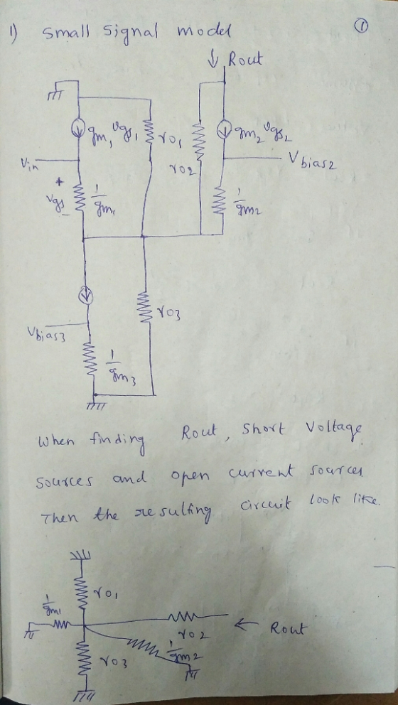
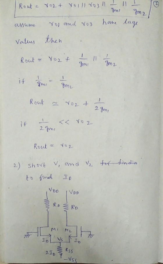
1. Find the output resistance of the folded cascode shown below, in...
2. For the amplifiers below, not all the bias details are shown. For the circuit on the left, what is the small signal...
 2. For the amplifiers below, not all the bias details are shown. For the circuit on the left, what is the small signal resistance looking into the a. source of M2 (Ri2)? b. Using part a, Find the voltage gain at the drain of Mi, and the total gain at the output. For the circuit on the right, known as a cascode amplifier, find the voltage gain. c. Express your answers in terms of the transistors gm, and RD. Assume...
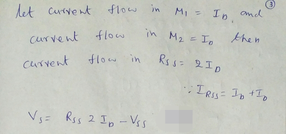
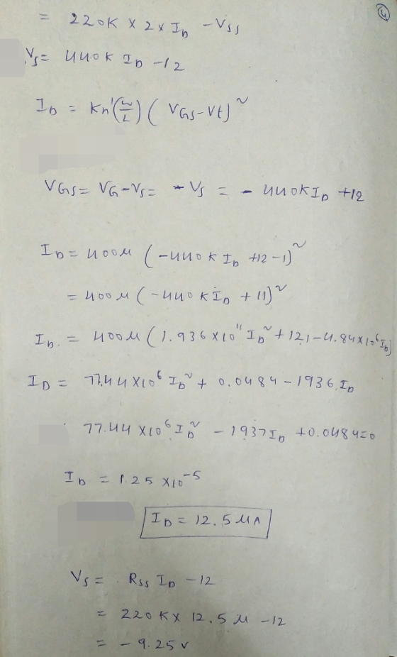
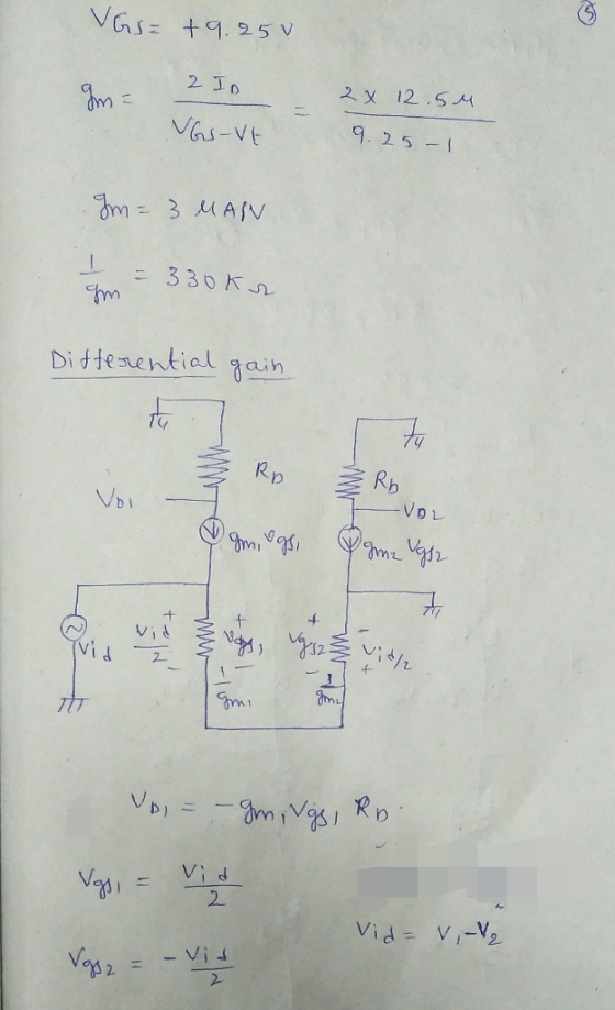
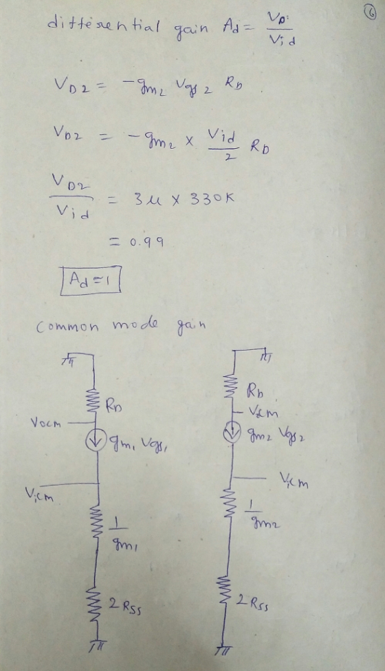
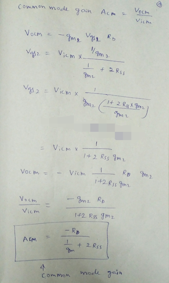
4) Consider the MOSFET differential amplifier shown below, with Io-2 mA, and RL- 10 kS2, Rss-100 ...
 4) Consider the MOSFET differential amplifier shown below, with Io-2 mA, and RL- 10 kS2, Rss-100 k2, VDD- +8V and Vss--8V. The NMOS transistors in the circuit are nominally identical, with kn 2 mA/V2, VTn 1.0 V and ro 100 k2. The PMoS transistors in the circuit are nominally identical, with kp 2 mA/V2, [VTpl 1.0 V and ro 100 kΩ M3 M4 0 M1 M2 a) First consider the DC bias point. Assuming that the current mirror requires at...
5) Consider the Cascode amplifier shown below. For the NMOS transistors, kn 0.2 mA/V2, Vr,-0.5 V,...
 5) Consider the Cascode amplifier shown below. For the NMOS transistors, kn 0.2 mA/V2, Vr,-0.5 V, (W/L)-(W/L)2-5. VDD-GV and IBIAs= 1.0 mA. a) Assuming λ-0 for all transistors, find the required DC gate- source voltages of M1 and M2 (VGsı and VGs2, respectively) BIAS VD out b) Again assuming 0 M2 for all transistors, what is the minimum DC value of VouT for which the amplifier works in high-gain regime? (W/L)2 in M1 For parts c)-f), Assume -0.01 for all...
3. In the circuit shown below, the differential pair (Mand M2) is biased with a current miror that consists of M3, M and Rref. The circuit parameters are: VDD-3 V, Rre/-15 ka, RD = 20 ka, and RL-40 k...
 3. In the circuit shown below, the differential pair (Mand M2) is biased with a current miror that consists of M3, M and Rref. The circuit parameters are: VDD-3 V, Rre/-15 ka, RD = 20 ka, and RL-40 kn. The transistors 25 M, and M, are identicalwith()M and M, are identical with (The oh M and M4 are identical with = ·The other transistor parameters are: indox-: 0.1 m1A/V2,VTN-0.5 V, γ-0 (body effect coefficient) and λ 0 (channel length modulation...
Please answer clearly Question 2 The amplifier shown in Figure 2 has the following parameters: Kn(W/L)-1 mA/V2, V-1 V Determine a) Voltage gain (Vo/vi) b) Input resistance (R) c) Output resistance (R...
 Please answer clearly
Question 2 The amplifier shown in Figure 2 has the following parameters: Kn(W/L)-1 mA/V2, V-1 V Determine a) Voltage gain (Vo/vi) b) Input resistance (R) c) Output resistance (Ro) d) Maximum output voltage swing so as the amplifier stays in saturation mode. Assume VDD-20 V, R1-2.5 ΚΩ, R2-1KQ, R3-0.5 ΚΩ, R4-5 MQ, R5_1ΜΩ. R4 R1 R5 R2 Ro R3
Question 2 The amplifier shown in Figure 2 has the following parameters: Kn(W/L)-1 mA/V2, V-1 V Determine a)...
Please answer clearly
Question 2 The amplifier shown in Figure 2 has the following parameters: Kn(W/L)-1 mA/V2, V-1 V Determine a) Voltage gain (Vo/vi) b) Input resistance (R) c) Output resistance (Ro) d) Maximum output voltage swing so as the amplifier stays in saturation mode. Assume VDD-20 V, R1-2.5 ΚΩ, R2-1KQ, R3-0.5 ΚΩ, R4-5 MQ, R5_1ΜΩ. R4 R1 R5 R2 Ro R3
Question 2 The amplifier shown in Figure 2 has the following parameters: Kn(W/L)-1 mA/V2, V-1 V Determine a)...
Please answer in full detail, show all work. thank you FInd all the DC collector currents showing...
 please answer in full detail, show all work. thank you FInd all
the DC collector currents showing all work.
Reference First stage Second stage Output stage current cc (+15 V) 13A 12 13 B 14 19 27 Ω Out 18 | R10 = 40 kΩ 27 Ω Q2 39 kΩ In In l CC 30 pF REF 24 I 16 10 17 50 kΩ 100 Ω 024 50 kΩ VEE 15 v) Figure 13.14 The 741 op-amp circuit: Qu, Qi2,...
please answer in full detail, show all work. thank you FInd all
the DC collector currents showing all work.
Reference First stage Second stage Output stage current cc (+15 V) 13A 12 13 B 14 19 27 Ω Out 18 | R10 = 40 kΩ 27 Ω Q2 39 kΩ In In l CC 30 pF REF 24 I 16 10 17 50 kΩ 100 Ω 024 50 kΩ VEE 15 v) Figure 13.14 The 741 op-amp circuit: Qu, Qi2,...
3.1. For the BJT differential pair configuration shown below, assume the input transistor beta is very large. Then...
 3.1. For the BJT differential pair configuration shown below,
assume the input transistor beta is very large.
Then find the differential signal vd = vB1 − vB2 sufficient to
cause:
3.2. A differential amplifier resembling that below uses I =
200μA, RC = 10kohm and VCC = 3V. Assume beta is very large
3.4.For the emitter follower in the figure below, given VCC =
15 V, VEE = −15 V, RL = 1 kohm and beta = 100 for all...
3.1. For the BJT differential pair configuration shown below,
assume the input transistor beta is very large.
Then find the differential signal vd = vB1 − vB2 sufficient to
cause:
3.2. A differential amplifier resembling that below uses I =
200μA, RC = 10kohm and VCC = 3V. Assume beta is very large
3.4.For the emitter follower in the figure below, given VCC =
15 V, VEE = −15 V, RL = 1 kohm and beta = 100 for all...
 2. For the amplifiers below, not all the bias details are shown. For the circuit on the left, what is the small signal resistance looking into the a. source of M2 (Ri2)? b. Using part a, Find the voltage gain at the drain of Mi, and the total gain at the output. For the circuit on the right, known as a cascode amplifier, find the voltage gain. c. Express your answers in terms of the transistors gm, and RD. Assume...
 4) Consider the MOSFET differential amplifier shown below, with Io-2 mA, and RL- 10 kS2, Rss-100 k2, VDD- +8V and Vss--8V. The NMOS transistors in the circuit are nominally identical, with kn 2 mA/V2, VTn 1.0 V and ro 100 k2. The PMoS transistors in the circuit are nominally identical, with kp 2 mA/V2, [VTpl 1.0 V and ro 100 kΩ M3 M4 0 M1 M2 a) First consider the DC bias point. Assuming that the current mirror requires at...
 5) Consider the Cascode amplifier shown below. For the NMOS transistors, kn 0.2 mA/V2, Vr,-0.5 V, (W/L)-(W/L)2-5. VDD-GV and IBIAs= 1.0 mA. a) Assuming λ-0 for all transistors, find the required DC gate- source voltages of M1 and M2 (VGsı and VGs2, respectively) BIAS VD out b) Again assuming 0 M2 for all transistors, what is the minimum DC value of VouT for which the amplifier works in high-gain regime? (W/L)2 in M1 For parts c)-f), Assume -0.01 for all...
 3. In the circuit shown below, the differential pair (Mand M2) is biased with a current miror that consists of M3, M and Rref. The circuit parameters are: VDD-3 V, Rre/-15 ka, RD = 20 ka, and RL-40 kn. The transistors 25 M, and M, are identicalwith()M and M, are identical with (The oh M and M4 are identical with = ·The other transistor parameters are: indox-: 0.1 m1A/V2,VTN-0.5 V, γ-0 (body effect coefficient) and λ 0 (channel length modulation...
 Please answer clearly
Question 2 The amplifier shown in Figure 2 has the following parameters: Kn(W/L)-1 mA/V2, V-1 V Determine a) Voltage gain (Vo/vi) b) Input resistance (R) c) Output resistance (Ro) d) Maximum output voltage swing so as the amplifier stays in saturation mode. Assume VDD-20 V, R1-2.5 ΚΩ, R2-1KQ, R3-0.5 ΚΩ, R4-5 MQ, R5_1ΜΩ. R4 R1 R5 R2 Ro R3
Question 2 The amplifier shown in Figure 2 has the following parameters: Kn(W/L)-1 mA/V2, V-1 V Determine a)...
Please answer clearly
Question 2 The amplifier shown in Figure 2 has the following parameters: Kn(W/L)-1 mA/V2, V-1 V Determine a) Voltage gain (Vo/vi) b) Input resistance (R) c) Output resistance (Ro) d) Maximum output voltage swing so as the amplifier stays in saturation mode. Assume VDD-20 V, R1-2.5 ΚΩ, R2-1KQ, R3-0.5 ΚΩ, R4-5 MQ, R5_1ΜΩ. R4 R1 R5 R2 Ro R3
Question 2 The amplifier shown in Figure 2 has the following parameters: Kn(W/L)-1 mA/V2, V-1 V Determine a)...
 please answer in full detail, show all work. thank you FInd all
the DC collector currents showing all work.
Reference First stage Second stage Output stage current cc (+15 V) 13A 12 13 B 14 19 27 Ω Out 18 | R10 = 40 kΩ 27 Ω Q2 39 kΩ In In l CC 30 pF REF 24 I 16 10 17 50 kΩ 100 Ω 024 50 kΩ VEE 15 v) Figure 13.14 The 741 op-amp circuit: Qu, Qi2,...
please answer in full detail, show all work. thank you FInd all
the DC collector currents showing all work.
Reference First stage Second stage Output stage current cc (+15 V) 13A 12 13 B 14 19 27 Ω Out 18 | R10 = 40 kΩ 27 Ω Q2 39 kΩ In In l CC 30 pF REF 24 I 16 10 17 50 kΩ 100 Ω 024 50 kΩ VEE 15 v) Figure 13.14 The 741 op-amp circuit: Qu, Qi2,...
 3.1. For the BJT differential pair configuration shown below,
assume the input transistor beta is very large.
Then find the differential signal vd = vB1 − vB2 sufficient to
cause:
3.2. A differential amplifier resembling that below uses I =
200μA, RC = 10kohm and VCC = 3V. Assume beta is very large
3.4.For the emitter follower in the figure below, given VCC =
15 V, VEE = −15 V, RL = 1 kohm and beta = 100 for all...
3.1. For the BJT differential pair configuration shown below,
assume the input transistor beta is very large.
Then find the differential signal vd = vB1 − vB2 sufficient to
cause:
3.2. A differential amplifier resembling that below uses I =
200μA, RC = 10kohm and VCC = 3V. Assume beta is very large
3.4.For the emitter follower in the figure below, given VCC =
15 V, VEE = −15 V, RL = 1 kohm and beta = 100 for all...
Most questions answered within 3 hours.
-
You purchase your daily coffee at the Chemist’s Coffeehouse and
have a choice of two cups:...
asked 1 hour ago -
Which of the following pairs of chemicals could be used to make
a buffer solution?
A.)...
asked 1 hour ago -
Problem 16-51 Sales
Activity Variance (LO 16-3)Odessa, Inc., reports the following
information concerning operations for the...
asked 2 hours ago -
Pictured on the right are thee point charges Q1 = 18.4 μC, Q2 =
-30.6 μC,...
asked 2 hours ago -
A graduate student is conducting research in psychology and
needs to obtain the IQ scores of...
asked 2 hours ago -
R2.84: There are 2 defective products in a production lot of 10.
An inspector randomly selected...
asked 4 hours ago -
Consider the following equilibrium system: COCl2(g) CO(g) +
Cl2(g) A 10.00 L evacuated flask is filled...
asked 4 hours ago -
1) What are the two distinct steps that one needs to perform
when developing a data...
asked 4 hours ago -
2) Write a C++ program that uses a class called “Degree” to
obtain the trigonometric
values...
asked 5 hours ago -
1. In eukaryotic cells the genomes of
&
asked 5 hours ago -
The standard enthalpy of propanol (C3H7OH) is -303.0 kJ/mol.
Compute both of the
gross and net...
asked 5 hours ago -
Why PWM using H-bridge for control motor speed is more power
effiecient than the linear amplifier...
asked 6 hours ago