


D Question 4 1 pts Consider practice question 3.4. The resistor RL is changed to 1.2 kilo-ohms. Solve part (a) of the question to find resistor R in kilo-ohms. Question 5 1 pts Consider the circuit in practice question 3.5. If the input voltage vi-2.5 volts, what is the output voltage vo?
Rc ic1 c2 E1 E2 ぶ!
Rc Rc + Vo - Q2 Q1 Ud
Vcc Ol VBE 2 Q2 Ri 03 VEE ЕЕ
QP RL
Homework Answers

Add Answer to:
3.1. For the BJT differential pair configuration shown below, assume the input transistor beta is very large. Then...
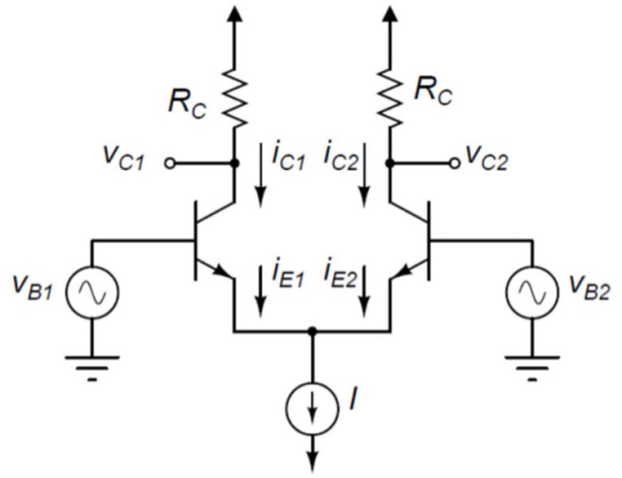
3.2. A differential amplifier resembling that below uses I = 200LA, Rç = 10k and Vcc = 3V. Assume very large. is What i...
 3.2. A differential amplifier resembling that below uses I = 200LA, Rç = 10k and Vcc = 3V. Assume very large. is What is the differential gain vva achieved for outputs taken differentially? What if single-ended outputs are taken from either collector? What is the upper limit of the common-mode input voltage for which operation keeps both transistors in the active mode? (c) Vec Rc Rc Q2 O D Question 2 1 pts Consider practice question 3.2. The bias current...
It is just the question 4 needs to be solved. Mind the changes in question 4. Question 4 1 pts Consider practice questio...
 It is just the question 4
needs to be solved. Mind the changes in question 4.
Question 4 1 pts Consider practice question 3.4. The resistor RL is changed to 1.9 kilo-ohms. Solve part (a) of the question to find resistor R in kilo-ohms. 3.4. For the emitter follower in the figure below, given Vcc = 15 V, Vee=-15 V, Ri = 1 kQ and B= 100 for all the transistors. In the following calculations assume VCEsat= 0.2 V and...
It is just the question 4
needs to be solved. Mind the changes in question 4.
Question 4 1 pts Consider practice question 3.4. The resistor RL is changed to 1.9 kilo-ohms. Solve part (a) of the question to find resistor R in kilo-ohms. 3.4. For the emitter follower in the figure below, given Vcc = 15 V, Vee=-15 V, Ri = 1 kQ and B= 100 for all the transistors. In the following calculations assume VCEsat= 0.2 V and...
circuit 3.4 Circuit 3.5 D Question 4 1 pts Consider practice question 3.4. The resistor RL is changed to 1.0 kilo-ohm...
 circuit 3.4
Circuit 3.5
D Question 4 1 pts Consider practice question 3.4. The resistor RL is changed to 1.0 kilo-ohms. Solve part (a) of the question to find resistor R in kilo-ohms. D Question 5 1 pts Consider the circuit in practice question 3.5. If the input voltage vi =-29 volts, what is the output voltage vo? VBE 7 We were unable to transcribe this image
D Question 4 1 pts Consider practice question 3.4. The resistor RL is...
circuit 3.4
Circuit 3.5
D Question 4 1 pts Consider practice question 3.4. The resistor RL is changed to 1.0 kilo-ohms. Solve part (a) of the question to find resistor R in kilo-ohms. D Question 5 1 pts Consider the circuit in practice question 3.5. If the input voltage vi =-29 volts, what is the output voltage vo? VBE 7 We were unable to transcribe this image
D Question 4 1 pts Consider practice question 3.4. The resistor RL is...
For the differential input stage shown below, the differential input impedance is required to be 100k....
 For the differential input stage shown below, the differential input impedance is required to be 100k. Estimate the bias current in the differential amplifier to meet this specification. Hence calculate the value of R2 (in ko) required to set this bias current. The Early voltage of the NPN transistor is 150 V and that for the PNP is 50 V. Vcc (+9 V) 2N2907 Q5 2N2907 Vin (-) Q6 2N2907 2N2907 Q8 2N2222 09 2N2222 VEE (-9 V) assume lo...
Given below is a differential operational amplifier in block form and its internal transistor circuit with...
 Given below is a differential operational amplifier in block
form and its internal transistor circuit with VCC=20V, VEE= 12 V ,
RC=5kΩ,RE=1kΩ and R1=2kΩ. Assume that the transistors are identical
and have a βac=βdc=100. An ac signal Vi(t)=5sin(10t) is applied to
the input terminals where Terminal 1 is Positive (non-invertinq)
& Terminal 2 is negative (inverting) as stated in the cases
below. Draw the output signals in each case.
: a) V1=Vi(t) , V2=Grounded. Vo(t)=Vo2-Vo1 )
b) V1=Grounded , V2=Vi(t)....
Given below is a differential operational amplifier in block
form and its internal transistor circuit with VCC=20V, VEE= 12 V ,
RC=5kΩ,RE=1kΩ and R1=2kΩ. Assume that the transistors are identical
and have a βac=βdc=100. An ac signal Vi(t)=5sin(10t) is applied to
the input terminals where Terminal 1 is Positive (non-invertinq)
& Terminal 2 is negative (inverting) as stated in the cases
below. Draw the output signals in each case.
: a) V1=Vi(t) , V2=Grounded. Vo(t)=Vo2-Vo1 )
b) V1=Grounded , V2=Vi(t)....
Design a BJT amplifier based on the specifications provided in the table below. Your design shoul...
 THE STEPS TO DO SO:
Design a BJT amplifier based on the specifications provided in the table below. Your design should be insensitive to β variations, and both the input and the output should be AC coupled as in Fig. 1. Supply Voltage, Vcc Load Resistance, RL Transistor's Current Gain, β Relative Variation of lc for VBE-0.7 ± 0.1 V 0-to-Peak Output Swing, Vo Voltage Gain, A Input Resistance, R THD for 5kHz IV (0-to-peak) Sine Wave Output Voltage, V。S5%...
THE STEPS TO DO SO:
Design a BJT amplifier based on the specifications provided in the table below. Your design should be insensitive to β variations, and both the input and the output should be AC coupled as in Fig. 1. Supply Voltage, Vcc Load Resistance, RL Transistor's Current Gain, β Relative Variation of lc for VBE-0.7 ± 0.1 V 0-to-Peak Output Swing, Vo Voltage Gain, A Input Resistance, R THD for 5kHz IV (0-to-peak) Sine Wave Output Voltage, V。S5%...
Q2) Please show all working Thank you :) Question 2 (25 Marks) (a) (6 Marks) Bias...
 Q2)
Please show all working
Thank you :)
Question 2 (25 Marks) (a) (6 Marks) Bias the CE amplifier in Figure 2 to have IE = 1mA. Assume B-100, VBE(On) = 0.7 V, Vcc = 15V, VEE= -15V and RB = 100kQ. List all node voltages, currents and resistor values. (b) (10 Marks) Draw the small-signal model for the CE amplifier in Figure 2 Determine the input resistance, output resistance and gain of the amplifier. Assume VA = 100V, RL...
Q2)
Please show all working
Thank you :)
Question 2 (25 Marks) (a) (6 Marks) Bias the CE amplifier in Figure 2 to have IE = 1mA. Assume B-100, VBE(On) = 0.7 V, Vcc = 15V, VEE= -15V and RB = 100kQ. List all node voltages, currents and resistor values. (b) (10 Marks) Draw the small-signal model for the CE amplifier in Figure 2 Determine the input resistance, output resistance and gain of the amplifier. Assume VA = 100V, RL...
4) Consider the MOSFET differential amplifier shown below, with Io-2 mA, and RL- 10 kS2, Rss-100 ...
 4) Consider the MOSFET differential amplifier shown below, with Io-2 mA, and RL- 10 kS2, Rss-100 k2, VDD- +8V and Vss--8V. The NMOS transistors in the circuit are nominally identical, with kn 2 mA/V2, VTn 1.0 V and ro 100 k2. The PMoS transistors in the circuit are nominally identical, with kp 2 mA/V2, [VTpl 1.0 V and ro 100 kΩ M3 M4 0 M1 M2 a) First consider the DC bias point. Assuming that the current mirror requires at...
4. Consider the BJT cascade amplifier shown below Vcc 18V R1 3.3ko 15uF r Vo RL...
 4. Consider the BJT cascade amplifier shown below Vcc 18V R1 3.3ko 15uF r Vo RL B 150 Rsa 500? 56k? Vi B 150 C1 CE 2.2k? a) Find the DC collector current (approximately the same in both transistors). b) Find the input impedance, output impedance, and no-load voltage gain. c) Find the Av, Avs, and Ai d) Estimate the lower cutoff frequency e) Why does this amplifier have better high-frequency performance thana common-emitter built using the same type of...
i just need help with B, C, D 3) (24 pts) The BJT amplifier shown below....
 i just need help with B, C, D
3) (24 pts) The BJT amplifier shown below. Please answer the following questions. Consider that B=150 VBE=0.75 V and VT-25mV a) What type of amplifier is this? (Select One) CE CE with RE CB b) Find the DC collector current Ic c) Find the transconductance gain gm d) Find the internal small signal voltage gain Au e) Find the input resistance of the small signal amplifier 1) Find the output resistance of...
i just need help with B, C, D
3) (24 pts) The BJT amplifier shown below. Please answer the following questions. Consider that B=150 VBE=0.75 V and VT-25mV a) What type of amplifier is this? (Select One) CE CE with RE CB b) Find the DC collector current Ic c) Find the transconductance gain gm d) Find the internal small signal voltage gain Au e) Find the input resistance of the small signal amplifier 1) Find the output resistance of...
 3.2. A differential amplifier resembling that below uses I = 200LA, Rç = 10k and Vcc = 3V. Assume very large. is What is the differential gain vva achieved for outputs taken differentially? What if single-ended outputs are taken from either collector? What is the upper limit of the common-mode input voltage for which operation keeps both transistors in the active mode? (c) Vec Rc Rc Q2 O D Question 2 1 pts Consider practice question 3.2. The bias current...
 It is just the question 4
needs to be solved. Mind the changes in question 4.
Question 4 1 pts Consider practice question 3.4. The resistor RL is changed to 1.9 kilo-ohms. Solve part (a) of the question to find resistor R in kilo-ohms. 3.4. For the emitter follower in the figure below, given Vcc = 15 V, Vee=-15 V, Ri = 1 kQ and B= 100 for all the transistors. In the following calculations assume VCEsat= 0.2 V and...
It is just the question 4
needs to be solved. Mind the changes in question 4.
Question 4 1 pts Consider practice question 3.4. The resistor RL is changed to 1.9 kilo-ohms. Solve part (a) of the question to find resistor R in kilo-ohms. 3.4. For the emitter follower in the figure below, given Vcc = 15 V, Vee=-15 V, Ri = 1 kQ and B= 100 for all the transistors. In the following calculations assume VCEsat= 0.2 V and...
 circuit 3.4
Circuit 3.5
D Question 4 1 pts Consider practice question 3.4. The resistor RL is changed to 1.0 kilo-ohms. Solve part (a) of the question to find resistor R in kilo-ohms. D Question 5 1 pts Consider the circuit in practice question 3.5. If the input voltage vi =-29 volts, what is the output voltage vo? VBE 7 We were unable to transcribe this image
D Question 4 1 pts Consider practice question 3.4. The resistor RL is...
circuit 3.4
Circuit 3.5
D Question 4 1 pts Consider practice question 3.4. The resistor RL is changed to 1.0 kilo-ohms. Solve part (a) of the question to find resistor R in kilo-ohms. D Question 5 1 pts Consider the circuit in practice question 3.5. If the input voltage vi =-29 volts, what is the output voltage vo? VBE 7 We were unable to transcribe this image
D Question 4 1 pts Consider practice question 3.4. The resistor RL is...
 For the differential input stage shown below, the differential input impedance is required to be 100k. Estimate the bias current in the differential amplifier to meet this specification. Hence calculate the value of R2 (in ko) required to set this bias current. The Early voltage of the NPN transistor is 150 V and that for the PNP is 50 V. Vcc (+9 V) 2N2907 Q5 2N2907 Vin (-) Q6 2N2907 2N2907 Q8 2N2222 09 2N2222 VEE (-9 V) assume lo...
 Given below is a differential operational amplifier in block
form and its internal transistor circuit with VCC=20V, VEE= 12 V ,
RC=5kΩ,RE=1kΩ and R1=2kΩ. Assume that the transistors are identical
and have a βac=βdc=100. An ac signal Vi(t)=5sin(10t) is applied to
the input terminals where Terminal 1 is Positive (non-invertinq)
& Terminal 2 is negative (inverting) as stated in the cases
below. Draw the output signals in each case.
: a) V1=Vi(t) , V2=Grounded. Vo(t)=Vo2-Vo1 )
b) V1=Grounded , V2=Vi(t)....
Given below is a differential operational amplifier in block
form and its internal transistor circuit with VCC=20V, VEE= 12 V ,
RC=5kΩ,RE=1kΩ and R1=2kΩ. Assume that the transistors are identical
and have a βac=βdc=100. An ac signal Vi(t)=5sin(10t) is applied to
the input terminals where Terminal 1 is Positive (non-invertinq)
& Terminal 2 is negative (inverting) as stated in the cases
below. Draw the output signals in each case.
: a) V1=Vi(t) , V2=Grounded. Vo(t)=Vo2-Vo1 )
b) V1=Grounded , V2=Vi(t)....
 THE STEPS TO DO SO:
Design a BJT amplifier based on the specifications provided in the table below. Your design should be insensitive to β variations, and both the input and the output should be AC coupled as in Fig. 1. Supply Voltage, Vcc Load Resistance, RL Transistor's Current Gain, β Relative Variation of lc for VBE-0.7 ± 0.1 V 0-to-Peak Output Swing, Vo Voltage Gain, A Input Resistance, R THD for 5kHz IV (0-to-peak) Sine Wave Output Voltage, V。S5%...
THE STEPS TO DO SO:
Design a BJT amplifier based on the specifications provided in the table below. Your design should be insensitive to β variations, and both the input and the output should be AC coupled as in Fig. 1. Supply Voltage, Vcc Load Resistance, RL Transistor's Current Gain, β Relative Variation of lc for VBE-0.7 ± 0.1 V 0-to-Peak Output Swing, Vo Voltage Gain, A Input Resistance, R THD for 5kHz IV (0-to-peak) Sine Wave Output Voltage, V。S5%...
 Q2)
Please show all working
Thank you :)
Question 2 (25 Marks) (a) (6 Marks) Bias the CE amplifier in Figure 2 to have IE = 1mA. Assume B-100, VBE(On) = 0.7 V, Vcc = 15V, VEE= -15V and RB = 100kQ. List all node voltages, currents and resistor values. (b) (10 Marks) Draw the small-signal model for the CE amplifier in Figure 2 Determine the input resistance, output resistance and gain of the amplifier. Assume VA = 100V, RL...
Q2)
Please show all working
Thank you :)
Question 2 (25 Marks) (a) (6 Marks) Bias the CE amplifier in Figure 2 to have IE = 1mA. Assume B-100, VBE(On) = 0.7 V, Vcc = 15V, VEE= -15V and RB = 100kQ. List all node voltages, currents and resistor values. (b) (10 Marks) Draw the small-signal model for the CE amplifier in Figure 2 Determine the input resistance, output resistance and gain of the amplifier. Assume VA = 100V, RL...
 4) Consider the MOSFET differential amplifier shown below, with Io-2 mA, and RL- 10 kS2, Rss-100 k2, VDD- +8V and Vss--8V. The NMOS transistors in the circuit are nominally identical, with kn 2 mA/V2, VTn 1.0 V and ro 100 k2. The PMoS transistors in the circuit are nominally identical, with kp 2 mA/V2, [VTpl 1.0 V and ro 100 kΩ M3 M4 0 M1 M2 a) First consider the DC bias point. Assuming that the current mirror requires at...
 4. Consider the BJT cascade amplifier shown below Vcc 18V R1 3.3ko 15uF r Vo RL B 150 Rsa 500? 56k? Vi B 150 C1 CE 2.2k? a) Find the DC collector current (approximately the same in both transistors). b) Find the input impedance, output impedance, and no-load voltage gain. c) Find the Av, Avs, and Ai d) Estimate the lower cutoff frequency e) Why does this amplifier have better high-frequency performance thana common-emitter built using the same type of...
 i just need help with B, C, D
3) (24 pts) The BJT amplifier shown below. Please answer the following questions. Consider that B=150 VBE=0.75 V and VT-25mV a) What type of amplifier is this? (Select One) CE CE with RE CB b) Find the DC collector current Ic c) Find the transconductance gain gm d) Find the internal small signal voltage gain Au e) Find the input resistance of the small signal amplifier 1) Find the output resistance of...
i just need help with B, C, D
3) (24 pts) The BJT amplifier shown below. Please answer the following questions. Consider that B=150 VBE=0.75 V and VT-25mV a) What type of amplifier is this? (Select One) CE CE with RE CB b) Find the DC collector current Ic c) Find the transconductance gain gm d) Find the internal small signal voltage gain Au e) Find the input resistance of the small signal amplifier 1) Find the output resistance of...
Most questions answered within 3 hours.
-
D. A student completed 20 courses in the School of Arts and
Sciences. Her grades in...
asked 51 minutes ago -
teo
pucks moving on a frictionless air table are about to collide. the
1.5 kg puck...
asked 56 minutes ago -
Problem #1
The area between Z = 0 and Z = 2.50
The area between Z...
asked 2 hours ago -
1. What is the meaning of the term communication style?
2. What are the benefits to...
asked 1 hour ago -
9.) You are buying a car that cost $26,500. You make payments of
$412 each month...
asked 2 hours ago -
. Suppose a discrete random variable has probability
distribution
P(x) = .2 if x = 0...
asked 3 hours ago -
Under the influence of its drive force, a snowmobile is moving
at a constant velocity along...
asked 4 hours ago -
Why do organizations decline? What steps can top
management take to halt, decline, and restore organizational...
asked 3 hours ago -
What mechanisms Drive speciation??
(I.e. what was Dawins theory on the orgin of species, and how...
asked 5 hours ago -
The manager at a car assembly plant believes that the mean
assembly time for a car...
asked 6 hours ago -
Which of the following is true of electron capture?
A) It decreases the nuclide's mass number...
asked 7 hours ago -
Assuming an efficiency of 43.10%, calculate the actual yield of
magnesium nitrate formed from 114.9 g...
asked 8 hours ago