
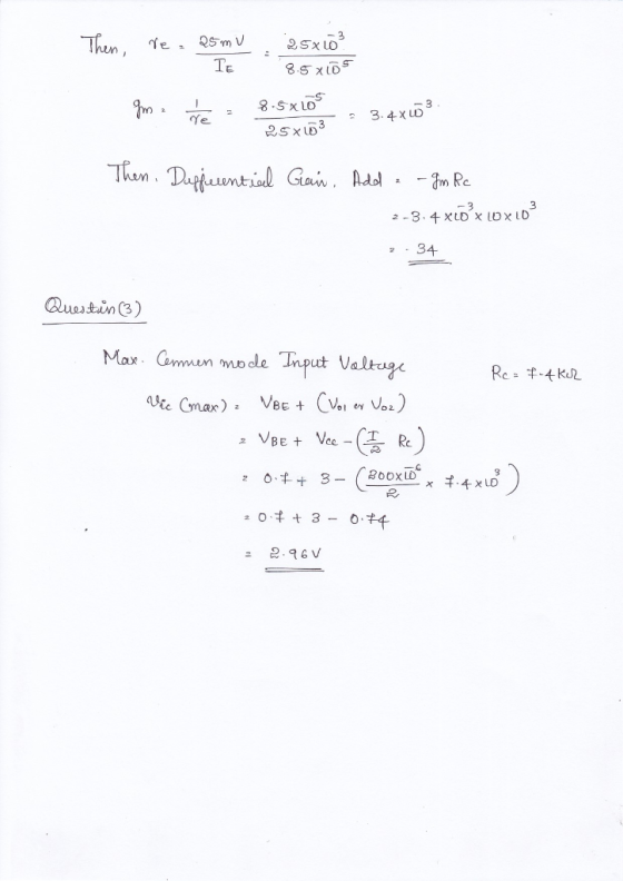
D Question 2 1 pts Consider practice question 3.2. The bias current I is changed to 0.17 mA. Find the differential gain in part (a). Question 3 1 pts Consider practice question 3.2 with the original value of bias current. The resistor is changed to 7.4 kilo-ohms. What is the maximum common-mode input voltage in part (c)?
Homework Answers


Add Answer to:
3.2. A differential amplifier resembling that below uses I = 200LA, Rç = 10k and Vcc = 3V. Assume very large. is What i...
3.1. For the BJT differential pair configuration shown below, assume the input transistor beta is very large. Then...
 3.1. For the BJT differential pair configuration shown below,
assume the input transistor beta is very large.
Then find the differential signal vd = vB1 − vB2 sufficient to
cause:
3.2. A differential amplifier resembling that below uses I =
200μA, RC = 10kohm and VCC = 3V. Assume beta is very large
3.4.For the emitter follower in the figure below, given VCC =
15 V, VEE = −15 V, RL = 1 kohm and beta = 100 for all...
3.1. For the BJT differential pair configuration shown below,
assume the input transistor beta is very large.
Then find the differential signal vd = vB1 − vB2 sufficient to
cause:
3.2. A differential amplifier resembling that below uses I =
200μA, RC = 10kohm and VCC = 3V. Assume beta is very large
3.4.For the emitter follower in the figure below, given VCC =
15 V, VEE = −15 V, RL = 1 kohm and beta = 100 for all...
The 1 mA. V, ls -VE -15 15 V, in the following differential amplifier circuit, Vcc parameters are given as β, 100, VBE# 0.7 V, pr-25 mV, K.-100 V. transistor Rc-10 kΩ For: RE-150 Ω Rc Rc REE-200...
 The 1 mA. V, ls -VE -15 15 V, in the following differential amplifier circuit, Vcc parameters are given as β, 100, VBE# 0.7 V, pr-25 mV, K.-100 V. transistor Rc-10 kΩ For: RE-150 Ω Rc Rc REE-200 kΩ a) What is the input differential resistance, Rid b) What is the overall voltage gain vV? You c) What is input common mode resistance, d) What is the worst case common mode gain that appear across the two input terminals? (4...
For the differential amplifier shown in Figure (2),
 For the differential amplifier shown in Figure (2),assume \(\mathrm{VCC}=12 \mathrm{~V}, \mathrm{VEE}=-12 \mathrm{~V}, \mathrm{Rc}=2 \mathrm{k} \Omega\), and \(\beta=100\) for all transistors.For the current source circuit (Transistor \(\left.Q_{3}\right): R_{1}=4 k \Omega, R_{2}=4 k \Omega, R_{3}=3 \mathrm{k} \Omega\), and \(r_{0}=100 \mathrm{k} \Omega\).a) In differential amplifier circuits, what do "well-matched transistors" mean?b) Why it is important to use well-matched transistors in differential amplifier circuits?c) What are the operating \(Q\) point values \(\left(I_{c Q}\right.\) and \(\left.V_{C Q}\right)\) for the transistors \(Q_{1}\) and \(Q_{2}\) ?d) Draw...
For the differential amplifier shown in Figure 6: Assume well-matched transistors and = 100 for all transistors: a) Wh...
 For the differential amplifier shown in Figure 6: Assume
well-matched transistors and = 100 for all transistors:
a) Why it is important to use well-matched transistors in
differential amplifier circuits? What is the potential influence of
mismatched transistors on the performance of the differential
amplifier?
b) Determine the resistor values (R1, R2 and R3) such that the
emitter coupled current IE = 0.5 mA and VC1 = 3 V.
c) Draw the ac equivalent circuit for the single ended...
For the differential amplifier shown in Figure 6: Assume
well-matched transistors and = 100 for all transistors:
a) Why it is important to use well-matched transistors in
differential amplifier circuits? What is the potential influence of
mismatched transistors on the performance of the differential
amplifier?
b) Determine the resistor values (R1, R2 and R3) such that the
emitter coupled current IE = 0.5 mA and VC1 = 3 V.
c) Draw the ac equivalent circuit for the single ended...
4) Consider the MOSFET differential amplifier shown below, with Io-2 mA, and RL- 10 kS2, Rss-100 ...
 4) Consider the MOSFET differential amplifier shown below, with Io-2 mA, and RL- 10 kS2, Rss-100 k2, VDD- +8V and Vss--8V. The NMOS transistors in the circuit are nominally identical, with kn 2 mA/V2, VTn 1.0 V and ro 100 k2. The PMoS transistors in the circuit are nominally identical, with kp 2 mA/V2, [VTpl 1.0 V and ro 100 kΩ M3 M4 0 M1 M2 a) First consider the DC bias point. Assuming that the current mirror requires at...
4. Consider the BJT cascade amplifier shown below Vcc 18V R1 3.3ko 15uF r Vo RL...
 4. Consider the BJT cascade amplifier shown below Vcc 18V R1 3.3ko 15uF r Vo RL B 150 Rsa 500? 56k? Vi B 150 C1 CE 2.2k? a) Find the DC collector current (approximately the same in both transistors). b) Find the input impedance, output impedance, and no-load voltage gain. c) Find the Av, Avs, and Ai d) Estimate the lower cutoff frequency e) Why does this amplifier have better high-frequency performance thana common-emitter built using the same type of...
i just need help with B, C, D 3) (24 pts) The BJT amplifier shown below....
 i just need help with B, C, D
3) (24 pts) The BJT amplifier shown below. Please answer the following questions. Consider that B=150 VBE=0.75 V and VT-25mV a) What type of amplifier is this? (Select One) CE CE with RE CB b) Find the DC collector current Ic c) Find the transconductance gain gm d) Find the internal small signal voltage gain Au e) Find the input resistance of the small signal amplifier 1) Find the output resistance of...
i just need help with B, C, D
3) (24 pts) The BJT amplifier shown below. Please answer the following questions. Consider that B=150 VBE=0.75 V and VT-25mV a) What type of amplifier is this? (Select One) CE CE with RE CB b) Find the DC collector current Ic c) Find the transconductance gain gm d) Find the internal small signal voltage gain Au e) Find the input resistance of the small signal amplifier 1) Find the output resistance of...
Electronics-common emmitter amplifier. Pls be try to be helpful Im trying to study here in this book example.. However im kinda lost and i cant follow the correct answers they got.. could someon...
 Electronics-common emmitter amplifier. Pls be try to be
helpful
Im trying to study here in this book example..
However im kinda lost and i cant follow the correct answers
they got.. could someone pls help me..
I just wanna learn this, i hope u can help me learn by showin
clear and corect solutions on how to properly got the
answer..
Also especially on finding the values on the laod line
analysis, im lost.
Pls help
Any helpful help would...
Electronics-common emmitter amplifier. Pls be try to be
helpful
Im trying to study here in this book example..
However im kinda lost and i cant follow the correct answers
they got.. could someone pls help me..
I just wanna learn this, i hope u can help me learn by showin
clear and corect solutions on how to properly got the
answer..
Also especially on finding the values on the laod line
analysis, im lost.
Pls help
Any helpful help would...
sedra smith book 7th edition chapter name is operational amplifier. question 12.1 to 12.10 I need...
 sedra smith book 7th edition chapter name is operational
amplifier. question 12.1 to 12.10 I need all solution with good
hand writing.
Problems 1075 Transistor Q3 WIL (um/um) 36/0.3 36/0.3 6/0.3 6/0.3 30/0.3 W/0.3 45/0.3 6/0.3 and A, if all devices are 0.3 m long, Q and Q2 are operated at overdrive voltages of 0.15-V magnitude, and Q is operated at Voy 0.2 V. Also, determine the op-amp output resistance 100 k2, C0.1 pF, G = 2 mA/V, R, =...
sedra smith book 7th edition chapter name is operational
amplifier. question 12.1 to 12.10 I need all solution with good
hand writing.
Problems 1075 Transistor Q3 WIL (um/um) 36/0.3 36/0.3 6/0.3 6/0.3 30/0.3 W/0.3 45/0.3 6/0.3 and A, if all devices are 0.3 m long, Q and Q2 are operated at overdrive voltages of 0.15-V magnitude, and Q is operated at Voy 0.2 V. Also, determine the op-amp output resistance 100 k2, C0.1 pF, G = 2 mA/V, R, =...
A common source amplifier circuit based on a single n-channel MOSFET is shown in Figure 4b. Assume that the transconductance gm-60 mS (equivalent to mA/ V) and drain source resistance, os,...
 A common source amplifier circuit based on a single n-channel MOSFET is shown in Figure 4b. Assume that the transconductance gm-60 mS (equivalent to mA/ V) and drain source resistance, os, is so large it may be neglected. 0) Calculate the open circuit voltage gain Av Yout/ Vis. i) The amplifier has a load of 10 k2. Determine the current gain Va. = 12 V 150k 4k3 Vout Vin 200k GND = 0 V Figure 4b a) State the name...
 3.1. For the BJT differential pair configuration shown below,
assume the input transistor beta is very large.
Then find the differential signal vd = vB1 − vB2 sufficient to
cause:
3.2. A differential amplifier resembling that below uses I =
200μA, RC = 10kohm and VCC = 3V. Assume beta is very large
3.4.For the emitter follower in the figure below, given VCC =
15 V, VEE = −15 V, RL = 1 kohm and beta = 100 for all...
3.1. For the BJT differential pair configuration shown below,
assume the input transistor beta is very large.
Then find the differential signal vd = vB1 − vB2 sufficient to
cause:
3.2. A differential amplifier resembling that below uses I =
200μA, RC = 10kohm and VCC = 3V. Assume beta is very large
3.4.For the emitter follower in the figure below, given VCC =
15 V, VEE = −15 V, RL = 1 kohm and beta = 100 for all...
 The 1 mA. V, ls -VE -15 15 V, in the following differential amplifier circuit, Vcc parameters are given as β, 100, VBE# 0.7 V, pr-25 mV, K.-100 V. transistor Rc-10 kΩ For: RE-150 Ω Rc Rc REE-200 kΩ a) What is the input differential resistance, Rid b) What is the overall voltage gain vV? You c) What is input common mode resistance, d) What is the worst case common mode gain that appear across the two input terminals? (4...
 For the differential amplifier shown in Figure 6: Assume
well-matched transistors and = 100 for all transistors:
a) Why it is important to use well-matched transistors in
differential amplifier circuits? What is the potential influence of
mismatched transistors on the performance of the differential
amplifier?
b) Determine the resistor values (R1, R2 and R3) such that the
emitter coupled current IE = 0.5 mA and VC1 = 3 V.
c) Draw the ac equivalent circuit for the single ended...
For the differential amplifier shown in Figure 6: Assume
well-matched transistors and = 100 for all transistors:
a) Why it is important to use well-matched transistors in
differential amplifier circuits? What is the potential influence of
mismatched transistors on the performance of the differential
amplifier?
b) Determine the resistor values (R1, R2 and R3) such that the
emitter coupled current IE = 0.5 mA and VC1 = 3 V.
c) Draw the ac equivalent circuit for the single ended...
 4) Consider the MOSFET differential amplifier shown below, with Io-2 mA, and RL- 10 kS2, Rss-100 k2, VDD- +8V and Vss--8V. The NMOS transistors in the circuit are nominally identical, with kn 2 mA/V2, VTn 1.0 V and ro 100 k2. The PMoS transistors in the circuit are nominally identical, with kp 2 mA/V2, [VTpl 1.0 V and ro 100 kΩ M3 M4 0 M1 M2 a) First consider the DC bias point. Assuming that the current mirror requires at...
 4. Consider the BJT cascade amplifier shown below Vcc 18V R1 3.3ko 15uF r Vo RL B 150 Rsa 500? 56k? Vi B 150 C1 CE 2.2k? a) Find the DC collector current (approximately the same in both transistors). b) Find the input impedance, output impedance, and no-load voltage gain. c) Find the Av, Avs, and Ai d) Estimate the lower cutoff frequency e) Why does this amplifier have better high-frequency performance thana common-emitter built using the same type of...
 i just need help with B, C, D
3) (24 pts) The BJT amplifier shown below. Please answer the following questions. Consider that B=150 VBE=0.75 V and VT-25mV a) What type of amplifier is this? (Select One) CE CE with RE CB b) Find the DC collector current Ic c) Find the transconductance gain gm d) Find the internal small signal voltage gain Au e) Find the input resistance of the small signal amplifier 1) Find the output resistance of...
i just need help with B, C, D
3) (24 pts) The BJT amplifier shown below. Please answer the following questions. Consider that B=150 VBE=0.75 V and VT-25mV a) What type of amplifier is this? (Select One) CE CE with RE CB b) Find the DC collector current Ic c) Find the transconductance gain gm d) Find the internal small signal voltage gain Au e) Find the input resistance of the small signal amplifier 1) Find the output resistance of...
 Electronics-common emmitter amplifier. Pls be try to be
helpful
Im trying to study here in this book example..
However im kinda lost and i cant follow the correct answers
they got.. could someone pls help me..
I just wanna learn this, i hope u can help me learn by showin
clear and corect solutions on how to properly got the
answer..
Also especially on finding the values on the laod line
analysis, im lost.
Pls help
Any helpful help would...
Electronics-common emmitter amplifier. Pls be try to be
helpful
Im trying to study here in this book example..
However im kinda lost and i cant follow the correct answers
they got.. could someone pls help me..
I just wanna learn this, i hope u can help me learn by showin
clear and corect solutions on how to properly got the
answer..
Also especially on finding the values on the laod line
analysis, im lost.
Pls help
Any helpful help would...
 sedra smith book 7th edition chapter name is operational
amplifier. question 12.1 to 12.10 I need all solution with good
hand writing.
Problems 1075 Transistor Q3 WIL (um/um) 36/0.3 36/0.3 6/0.3 6/0.3 30/0.3 W/0.3 45/0.3 6/0.3 and A, if all devices are 0.3 m long, Q and Q2 are operated at overdrive voltages of 0.15-V magnitude, and Q is operated at Voy 0.2 V. Also, determine the op-amp output resistance 100 k2, C0.1 pF, G = 2 mA/V, R, =...
sedra smith book 7th edition chapter name is operational
amplifier. question 12.1 to 12.10 I need all solution with good
hand writing.
Problems 1075 Transistor Q3 WIL (um/um) 36/0.3 36/0.3 6/0.3 6/0.3 30/0.3 W/0.3 45/0.3 6/0.3 and A, if all devices are 0.3 m long, Q and Q2 are operated at overdrive voltages of 0.15-V magnitude, and Q is operated at Voy 0.2 V. Also, determine the op-amp output resistance 100 k2, C0.1 pF, G = 2 mA/V, R, =...
 A common source amplifier circuit based on a single n-channel MOSFET is shown in Figure 4b. Assume that the transconductance gm-60 mS (equivalent to mA/ V) and drain source resistance, os, is so large it may be neglected. 0) Calculate the open circuit voltage gain Av Yout/ Vis. i) The amplifier has a load of 10 k2. Determine the current gain Va. = 12 V 150k 4k3 Vout Vin 200k GND = 0 V Figure 4b a) State the name...
Most questions answered within 3 hours.
-
python
Define a function called print_values which takes a dictionary
object as a parameter. The function...
asked 49 minutes ago -
In Chapter 1 you created a program named Triangle in
which you displayed a seven-line triangle...
asked 45 minutes ago -
Research question: What are the differences between separately
stated and non separately stated transactions in an...
asked 1 hour ago -
By using Arduino write a code that connects two LEDs to two
push-buttons. Each button controls...
asked 2 hours ago -
Bank of America has bonds that pay a coupon interest rate of 5.5
percent and mature...
asked 2 hours ago -
Problem: Patient Fees C++
You are to write a program that computes a patient’s bill for...
asked 4 hours ago -
In a population of interest, we know that, 77% drink coffee, and
23% drink tea. Assume...
asked 4 hours ago -
Given that f(x) = e-(x-1) for x > 1, determine the following
probabilities:
a) P(X <...
asked 4 hours ago -
A mechanic pushes a 2.60 ✕ 103-kg car from rest to a speed of v,
doing...
asked 4 hours ago -
International information systems result in all of the following
except:
A. improved quality of information flow....
asked 4 hours ago -
The president of the retailer Prime Products has just approached
the company’s bank with a request...
asked 4 hours ago -
If the carrying amount is $200,000 and recoverable amount is
$205000, the impairment amount is:
Select...
asked 4 hours ago