
Homework Answers


Add Answer to:
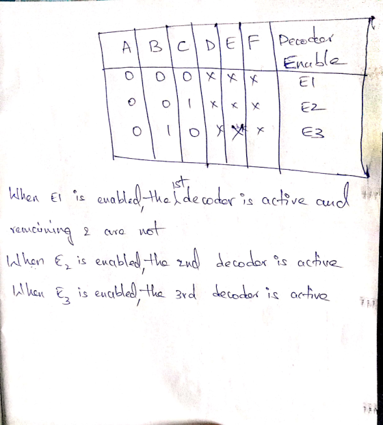
4. Design a 1-of-24 decoder using the shown 1-of -8 decoder. 12 points 74ALS138 1-01-8 decoder...
Design 4 to 1 mutiplexer using the design procedure : 8. Design 2 to 4 decoder...
Design 4 to 1 mutiplexer using the design procedure : 8. Design 2 to 4 decoder : 9. Design 4 bit comparator: 10. Design 1 bit ALU: 11. What is the difference between a combinational circuit and sequential circuit? Give example of each. 12. Draw an arduino board and label 10 major parts. 13. Describe the general setup for an arduino board when used to design a digital system.
Design a 32-input Mux using 8 and 4 input multiplexers. Design 4 to 16 decoder using...
 Design a 32-input Mux using 8 and 4 input multiplexers. Design 4 to 16 decoder using 3 to 8 decoders. 6.
Design 3- to – 8 decoder using logic gates with enabler, AND, NOT, etc..? Design 3- to – 8 decode...
Design 3- to – 8 decoder using logic gates with enabler, AND, NOT, etc..? Design 3- to – 8 decoder using only two 2-to-4 decoders graphical blocks, use enabler input? a) Design a 3-bit ripple-carry adder using AND, OR, NOT, EXOR, etc.; include carry-in (Cin), carry-out (Cout) and overflow input/output signals? Note: Design for 1-bit first, then extrapolate to 4-bit using 1-bit full-adder graphical block. Design a 3-bit ripple-carry subtractor using AND, OR, NOT, EXOR, etc..; include carry-in (Cin), carry-out...
12: Design a 2x4 decoder using only a minimum number of 2-bit magnitude comparators. The compleme...
 12: Design a 2x4 decoder using only a minimum number of 2-bit magnitude comparators. The complements of variables are not available, Logic levels 1 and 0 are accessible.
12: Design a 2x4 decoder using only a minimum number of 2-bit magnitude comparators. The complements of variables are not available, Logic levels 1 and 0 are accessible.
12: Design a 2x4 decoder using only a minimum number of 2-bit magnitude comparators. The complements of variables are not available, Logic levels 1 and 0 are accessible.
digital logic design 5. (20 Points) Given the logie circuit below, with the decoder having active...
 digital logic design
5. (20 Points) Given the logie circuit below, with the decoder having active low outputs as shown. Find the minimum switching expression for f(W,X,Y,Z) in the SOP form. Y EXY х w 4-6-16 10 Decoder GI 12 13P 14 150 I D G Search or type URL 5 6 & 7 8 9 0
digital logic design
5. (20 Points) Given the logie circuit below, with the decoder having active low outputs as shown. Find the minimum switching expression for f(W,X,Y,Z) in the SOP form. Y EXY х w 4-6-16 10 Decoder GI 12 13P 14 150 I D G Search or type URL 5 6 & 7 8 9 0
Design a dual 8-to-1 line multiplexer using a 3-to-8 line decoder and two 8X2 AND-ORS.
Design a dual 8-to-1 line multiplexer using a 3-to-8 line decoder and two 8X2 AND-ORS.
computer architecture 4. Design a 2-to-4-line decoder with enable using inverters 2to-4-line decoder vi AND gates...
 computer architecture
4. Design a 2-to-4-line decoder with enable using inverters 2to-4-line decoder vi AND gates and
computer architecture
4. Design a 2-to-4-line decoder with enable using inverters 2to-4-line decoder vi AND gates and
Do this in VHDL 8. Design the following 2-to-4 Decoder in VHDL
 Do this in VHDL
8. Design the following 2-to-4 Decoder in VHDL
Do this in VHDL
8. Design the following 2-to-4 Decoder in VHDL
Problem 1. Sequential Circuit Design Using a decoder and AND gates, implement a 4-input multiplexer. ....
 Problem 1. Sequential Circuit Design Using a decoder and AND gates, implement a 4-input multiplexer. . Using D-FFs, implement a 4-bit register. If using circuit verse, connect the Din signals to inputs blocks and connect Power to the enable lines. Do not forget the clock.
Design an address decoding using decoder (2 x 4). Consider, we wish to construct 1K byte...
 Design an address decoding using decoder (2 x 4). Consider, we wish to construct 1K byte memory using 4 RAM chips, having 8 bits address line.
 Design a 32-input Mux using 8 and 4 input multiplexers. Design 4 to 16 decoder using 3 to 8 decoders. 6.
 12: Design a 2x4 decoder using only a minimum number of 2-bit magnitude comparators. The complements of variables are not available, Logic levels 1 and 0 are accessible.
12: Design a 2x4 decoder using only a minimum number of 2-bit magnitude comparators. The complements of variables are not available, Logic levels 1 and 0 are accessible.
12: Design a 2x4 decoder using only a minimum number of 2-bit magnitude comparators. The complements of variables are not available, Logic levels 1 and 0 are accessible.
 digital logic design
5. (20 Points) Given the logie circuit below, with the decoder having active low outputs as shown. Find the minimum switching expression for f(W,X,Y,Z) in the SOP form. Y EXY х w 4-6-16 10 Decoder GI 12 13P 14 150 I D G Search or type URL 5 6 & 7 8 9 0
digital logic design
5. (20 Points) Given the logie circuit below, with the decoder having active low outputs as shown. Find the minimum switching expression for f(W,X,Y,Z) in the SOP form. Y EXY х w 4-6-16 10 Decoder GI 12 13P 14 150 I D G Search or type URL 5 6 & 7 8 9 0
 computer architecture
4. Design a 2-to-4-line decoder with enable using inverters 2to-4-line decoder vi AND gates and
computer architecture
4. Design a 2-to-4-line decoder with enable using inverters 2to-4-line decoder vi AND gates and
 Do this in VHDL
8. Design the following 2-to-4 Decoder in VHDL
Do this in VHDL
8. Design the following 2-to-4 Decoder in VHDL
 Problem 1. Sequential Circuit Design Using a decoder and AND gates, implement a 4-input multiplexer. . Using D-FFs, implement a 4-bit register. If using circuit verse, connect the Din signals to inputs blocks and connect Power to the enable lines. Do not forget the clock.
 Design an address decoding using decoder (2 x 4). Consider, we wish to construct 1K byte memory using 4 RAM chips, having 8 bits address line.
Most questions answered within 3 hours.
-
explain and comment out your answer
43. How many address lines are required to address a...
asked 3 minutes ago -
A sample of 45 observations is selected from a normal
population. The sample mean is 49,...
asked 18 minutes ago -
A construction company is planning to bid on a building
contract. The bid costs the company...
asked 15 minutes ago -
A firm operating in a purely competitive environment is faced
with a market price of $250....
asked 22 minutes ago -
•Let’s say someone claims the average population size is
600 feet squared and the housing authority...
asked 29 minutes ago -
Cynaide is a deadly poison that blocks the last step in the
electron transport chain of...
asked 34 minutes ago -
Your friend tells you that there is a vending machine on campus
that dispenses M&M packs...
asked 49 minutes ago -
What advantages are there to using piperidine rather than
hydroxide as a base?
asked 47 minutes ago -
7. The life of a Freeze Breeze electric fan is normally
distributed with a mean 4...
asked 50 minutes ago -
1. A 751 mL NaCl solution is diluted to a volume of 1.06 L and a...
asked 55 minutes ago -
8
A $20,000 face value STRIPS is currently quoted at 38.642 and
has 8 years to...
asked 56 minutes ago -
The current exchange rate between the Japanese yen and
the US dollar is 120 yen per...
asked 58 minutes ago