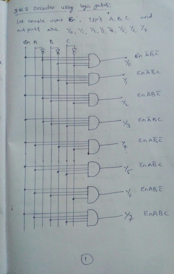
Design 3- to – 8 decoder using logic gates with enabler, AND, NOT, etc..? Design 3- to – 8 decode...
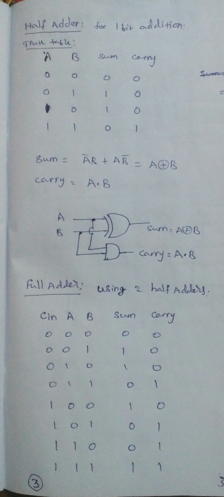
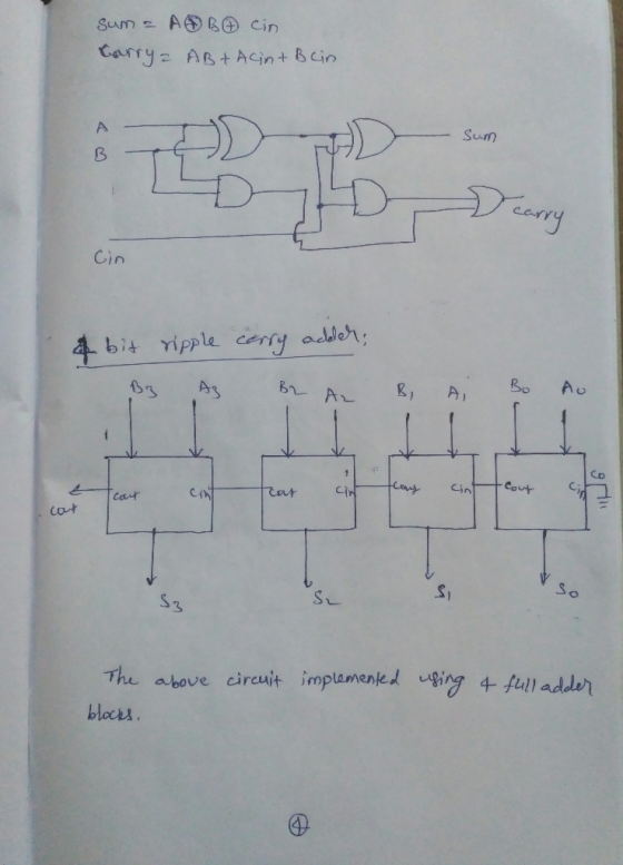
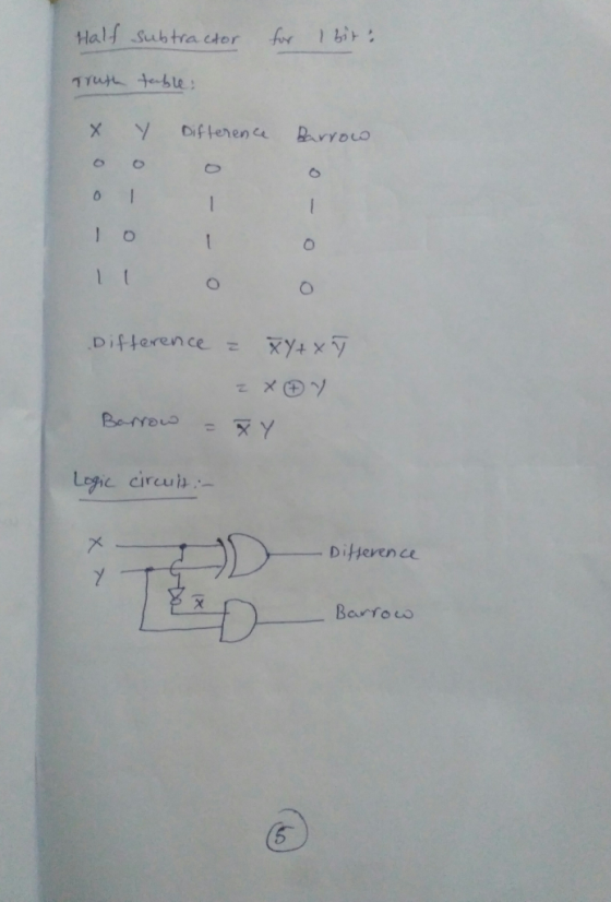
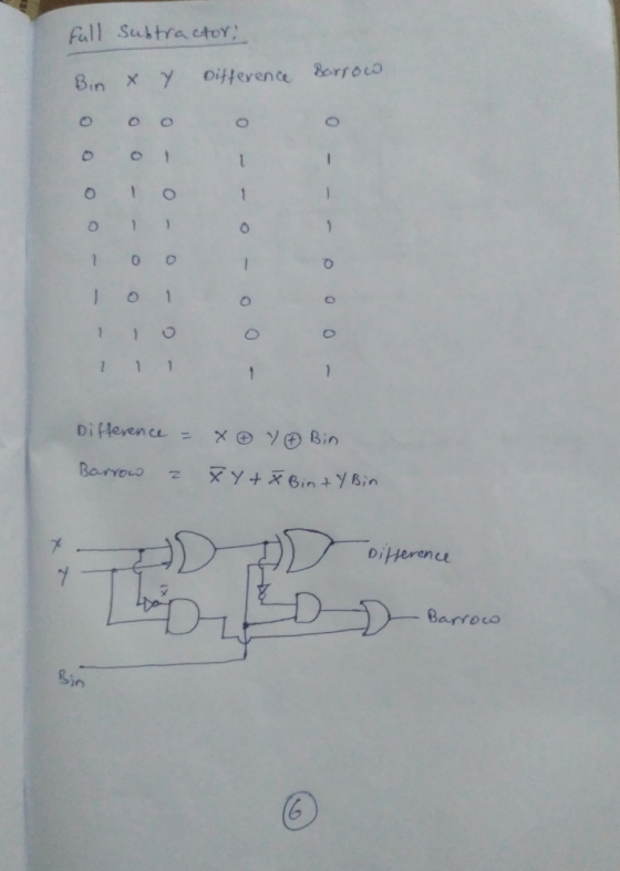
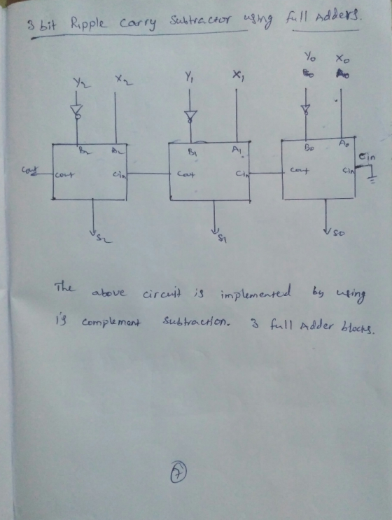
Design 3- to – 8 decoder using logic gates with enabler, AND, NOT, etc..? Design 3- to – 8 decoder using only two 2-to-4 decoders graphical blocks, use enabler input? a) Design a 3-bit ripple-carry adder using AND, OR, NOT, EXOR, etc.; include carry-in (Cin), carry-out (Cout) and overflow input/output signals? Note: Design for 1-bit first, then extrapolate to 4-bit using 1-bit full-adder graphical block. Design a 3-bit ripple-carry subtractor using AND, OR, NOT, EXOR, etc..; include carry-in (Cin), carry-out (Cout) and overflow input/output signals. Note: Design for 1-bit first, then extrapolate to 3-bit using functional block of 1-bit full-adder.
Homework Answers

Add Answer to:
Design 3- to – 8 decoder using logic gates with enabler, AND, NOT, etc..? Design 3- to – 8 decode...
Adder Design FAO FA1 B A Cin B Coub die los - S doo Problem 4.1...
 Adder Design FAO FA1 B A Cin B Coub die los - S doo Problem 4.1 (17 points) Design a fast 4 bit ripple-carry adder using the two full adder cells shown in Figure 4 and CMOS inverters. Label the inputs A[3:0), B(3:0), Cin and the outputs S(3:0) and Cout. Assume the delay through an inverter tiny = 4ps, the delay from any input to the full adder carry output is tc. = 7ps and to the sum output is...
number 4 and 5 please! PROBLEM STATEMENT A logic circuit is needed to add multi-bit binary...
 number 4 and 5 please!
PROBLEM STATEMENT A logic circuit is needed to add multi-bit binary numbers. A 2-level circuit that would add two four-bit numbers would have 9 inputs and five outputs. Although a 2-level SOP or POS circuit theoretically would be very fast, it has numerous drawbacks that make it impractical. The design would be very complex in terms of the number of logic gates. The number of inputs for each gate would challenge target technologies. Testing would...
number 4 and 5 please!
PROBLEM STATEMENT A logic circuit is needed to add multi-bit binary numbers. A 2-level circuit that would add two four-bit numbers would have 9 inputs and five outputs. Although a 2-level SOP or POS circuit theoretically would be very fast, it has numerous drawbacks that make it impractical. The design would be very complex in terms of the number of logic gates. The number of inputs for each gate would challenge target technologies. Testing would...
Building and testing basic combinational circuits using Verilog HDL Description: Build and test t...
Building and testing basic combinational circuits using Verilog HDL Description: Build and test the following circuits using gate-level modeling in Verilog HDL. 1. 3-input majority function. 2. Conditional inverter (see the table below: x - control input, y - data input). Do NOT use XOR gates for the implementation. x y Output 0 y 1 y' 3. Two-input multiplexer (see the table below: x,y - data inputs, z - control input). z Output 0 x 1 y 4. 1-bit half...
QUESTION 1 Suppose that an engineer wants to create a three bit adder using the method...
 QUESTION 1 Suppose that an engineer wants to create a three bit adder using the method described in Lecture 25. As part of the design process, the engineer creates the following building block component: a b Cin Full Adder Cout s In order to create the three bit adder, each of the three building blocks will need to be correctly connected together. In the circuit below, each of the possible connection points has been labeled with a number: A[2] 2...
Building and testing basic combinational circuits using Verilog HDL Description: Build and test the following circuits using gate-level modeling in Verilog HDL 1.3-input majority function 2.Condition...
 Building and testing basic combinational circuits using Verilog HDL Description: Build and test the following circuits using gate-level modeling in Verilog HDL 1.3-input majority function 2.Conditional inverter (see the table below: x - control input, y -data input). Do NOT use XOR gates for the implementation. Output 3. Two-input multiplexer (see the table below: x.y -data inputs, z- control input) Output 4. 1-bit half adder. 5. 1-bit full adder by cascading two half adders 6.1-bit full adder directly (as in...
(h) Using the following relationship: and the relationship determined in (h), design a 1-bit adde...
 (h) Using the following relationship: and the relationship determined in (h), design a 1-bit adder/subtractor circuit which has the following inputs: A, B, Sel and Cin/Bin D and outputs: S/D and Cout/Bout Where Sel is a selection line with the following properties Selection Operation 1 Subtractor Page 40 of 44 EEE2046F/EEE2050F Practical Manual 2019 (version 1.0) (Revision date: 2019-02-26) EEE2046F/EEE2050F Practical Manual Draw a full circuit diagram of the Boolean equation using 2-input logic gates and include it in your...
4. Design a four input EXOR gate using 3 X 8 decoders and extra gates.
 4. Design a four input EXOR gate using 3 X 8 decoders and extra gates.
(1) How do you design a 4-bit subtractor (i.e. C = A - B) using 1-bit...
(1) How do you design a 4-bit subtractor (i.e. C = A - B) using 1-bit full adders, and with circuits for overflow detection. (Note: output 1 if there is overflow; otherwise, output 0.)
Design a 32-input Mux using 8 and 4 input multiplexers. Design 4 to 16 decoder using...
 Design a 32-input Mux using 8 and 4 input multiplexers. Design 4 to 16 decoder using 3 to 8 decoders. 6.
Problem 1. Sequential Circuit Design Using a decoder and AND gates, implement a 4-input multiplexer. ....
 Problem 1. Sequential Circuit Design Using a decoder and AND gates, implement a 4-input multiplexer. . Using D-FFs, implement a 4-bit register. If using circuit verse, connect the Din signals to inputs blocks and connect Power to the enable lines. Do not forget the clock.
 Adder Design FAO FA1 B A Cin B Coub die los - S doo Problem 4.1 (17 points) Design a fast 4 bit ripple-carry adder using the two full adder cells shown in Figure 4 and CMOS inverters. Label the inputs A[3:0), B(3:0), Cin and the outputs S(3:0) and Cout. Assume the delay through an inverter tiny = 4ps, the delay from any input to the full adder carry output is tc. = 7ps and to the sum output is...
 number 4 and 5 please!
PROBLEM STATEMENT A logic circuit is needed to add multi-bit binary numbers. A 2-level circuit that would add two four-bit numbers would have 9 inputs and five outputs. Although a 2-level SOP or POS circuit theoretically would be very fast, it has numerous drawbacks that make it impractical. The design would be very complex in terms of the number of logic gates. The number of inputs for each gate would challenge target technologies. Testing would...
number 4 and 5 please!
PROBLEM STATEMENT A logic circuit is needed to add multi-bit binary numbers. A 2-level circuit that would add two four-bit numbers would have 9 inputs and five outputs. Although a 2-level SOP or POS circuit theoretically would be very fast, it has numerous drawbacks that make it impractical. The design would be very complex in terms of the number of logic gates. The number of inputs for each gate would challenge target technologies. Testing would...
 QUESTION 1 Suppose that an engineer wants to create a three bit adder using the method described in Lecture 25. As part of the design process, the engineer creates the following building block component: a b Cin Full Adder Cout s In order to create the three bit adder, each of the three building blocks will need to be correctly connected together. In the circuit below, each of the possible connection points has been labeled with a number: A[2] 2...
 Building and testing basic combinational circuits using Verilog HDL Description: Build and test the following circuits using gate-level modeling in Verilog HDL 1.3-input majority function 2.Conditional inverter (see the table below: x - control input, y -data input). Do NOT use XOR gates for the implementation. Output 3. Two-input multiplexer (see the table below: x.y -data inputs, z- control input) Output 4. 1-bit half adder. 5. 1-bit full adder by cascading two half adders 6.1-bit full adder directly (as in...
 (h) Using the following relationship: and the relationship determined in (h), design a 1-bit adder/subtractor circuit which has the following inputs: A, B, Sel and Cin/Bin D and outputs: S/D and Cout/Bout Where Sel is a selection line with the following properties Selection Operation 1 Subtractor Page 40 of 44 EEE2046F/EEE2050F Practical Manual 2019 (version 1.0) (Revision date: 2019-02-26) EEE2046F/EEE2050F Practical Manual Draw a full circuit diagram of the Boolean equation using 2-input logic gates and include it in your...
 4. Design a four input EXOR gate using 3 X 8 decoders and extra gates.
 Design a 32-input Mux using 8 and 4 input multiplexers. Design 4 to 16 decoder using 3 to 8 decoders. 6.
 Problem 1. Sequential Circuit Design Using a decoder and AND gates, implement a 4-input multiplexer. . Using D-FFs, implement a 4-bit register. If using circuit verse, connect the Din signals to inputs blocks and connect Power to the enable lines. Do not forget the clock.
Most questions answered within 3 hours.
-
Perform the following calculation. Make sure to pay attention to
significant figures. Your answer should be...
asked 8 minutes ago -
10. Net Present Value
Method and Internal Rate of Return Method for a service company
Buckeye...
asked 9 minutes ago -
An air conditioner removes hot air at 35 °C and 70 % relative
humidity from the...
asked 9 minutes ago -
TRUE OR FALSE :if false please explain
protiens folds up according to thermodynamic principles into a...
asked 12 minutes ago -
Of the 28 restaurants in an area, 4 serve on one type of
cuisine, 9 serve...
asked 27 minutes ago -
Which of the following is FALSE for catabolic pathways?
They are oxidative.
They generate oxidized enzyme...
asked 42 minutes ago -
Question 3 (20 Marks)
Read the text below and answer the question
accordingly.
ABC Enterprises Cc...
asked 48 minutes ago -
How does computer technology such as patient portals
affects revenue and expenses in a healthcare
environment?
asked 49 minutes ago -
what is the most stable chair conformation for beta -
D - Mannose
asked 50 minutes ago -
Use the definition of the fact that f(x) is O(g(x)) to
show that:
1. 7x^2 is...
asked 51 minutes ago -
In view of the fact that so many marriages end in divorce, why
do you think...
asked 1 hour ago -
You are an entrepreneur starting a biotechnology firm. If your
research is successful, the technology can...
asked 1 hour ago