
Homework Answers
Add Answer to:
6. Graphically determine the Q-point for the circuit in Figure 6(a) using the transfer characteristic curve...
5 Determine lo and Vas for the JFET with volage divder bas in Fiqure 5, gven...
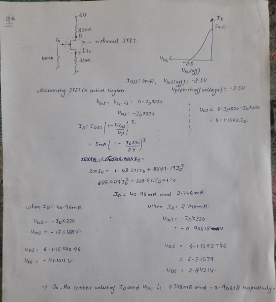
 5 Determine lo and Vas for the JFET with volage divder bas in Fiqure 5, gven that for this particular JFET the parameter values are such that Vo TV (B marks) Vco +12 V RD 68 MD 3.3 k RS R 10 MO 22 k Figure 5 6 Graphically determine the Q-point for the JFET crcut in Fqure Ba usng the trarsfer characteristic curve in Fiqure & (8 marks) Inss 5 mA Von +6 V RD 820 Rs 330 Ro...
The circuit 3-The circuit of problem # 2 is subjected to a small ac input by the signal generator. By neglecting the voltage drop across the coupling and bypass capacitors, determine the small signa...
 The circuit
3-The circuit of problem # 2 is subjected to a small ac input by the signal generator. By neglecting the voltage drop across the coupling and bypass capacitors, determine the small signal voltage gain Vo/ Vì = Avi , input resistance Ri-vi / ii and the output resistance Ro external to R Avi= Ri= , Ro The accompanying circuit shows a 4-resistor biased JFET transistor Determine the values of Rp and Rs so that the Q-point is equal...
The circuit
3-The circuit of problem # 2 is subjected to a small ac input by the signal generator. By neglecting the voltage drop across the coupling and bypass capacitors, determine the small signal voltage gain Vo/ Vì = Avi , input resistance Ri-vi / ii and the output resistance Ro external to R Avi= Ri= , Ro The accompanying circuit shows a 4-resistor biased JFET transistor Determine the values of Rp and Rs so that the Q-point is equal...
explain in detail B) Find the Q-point for the transistor in the circuit in Figure below...
 explain in detail
B) Find the Q-point for the transistor in the circuit in Figure below if Vpp = +12 V, K'n=0.1mA/V², VIN=0.75V, 20. (10pts) VpD 330 k2 10 M2 10
explain in detail
B) Find the Q-point for the transistor in the circuit in Figure below if Vpp = +12 V, K'n=0.1mA/V², VIN=0.75V, 20. (10pts) VpD 330 k2 10 M2 10
for the enhancement-type MOSFET circuit by plotting the 5. B) Determine IDo and transfer curve and...
 for the enhancement-type MOSFET circuit by plotting the 5. B) Determine IDo and transfer curve and then using load line analysis. VDSQ A lp-mA 12 11 9 12 V 8 Rp 2 kn 7- 6 1 pF Ra 10 MQ 3- IDce)-6 mA Vast-8 V Vasm-3 V &-20 uS 2 1 uF 9 10 11 12 (Von) 8 Vas a) k Ipso = VDSQ b) Using gos 20 uS i) Determine gm ii) Find ra iii) Calculate Z and Zo...
2. (25) You have been given an N-channel enhancement mode MOSFET to be used in the...
 2. (25) You have been given an N-channel enhancement mode MOSFET to be used in the next circuits. The NMOS has the characteristics of Ky = 1.0 mA/V,20, and Vin =1.0 V. A graph o current-voltage characteristics is shown on the next page of the test. (a) Determine resistor values (R. R. Ro Rs) so that Ipo = 4 mA and lose Let Ri= R/ || R 100 K and Vas Vs. Vpp = 12 V. VID = ID. RD"...
؟! ELE-2403 26. Given that the drain-to-ground voltage in Figure Electronics ADWC-HCT le drain-to-ground voltage in...
 ؟!
ELE-2403 26. Given that the drain-to-ground voltage in Figure Electronics ADWC-HCT le drain-to-ground voltage in Figure 8-71 is 5 V, determine the Q-point of the circuit. VOD +9 V 322 MA 27. Find the Q-point values for the JFET with voltage-divider bias in Figure 8-72. 'oss = 5 mA 3R 3RD 3.3 MO 1.8 WI Vas -4V Vasco
؟!
ELE-2403 26. Given that the drain-to-ground voltage in Figure Electronics ADWC-HCT le drain-to-ground voltage in Figure 8-71 is 5 V, determine the Q-point of the circuit. VOD +9 V 322 MA 27. Find the Q-point values for the JFET with voltage-divider bias in Figure 8-72. 'oss = 5 mA 3R 3RD 3.3 MO 1.8 WI Vas -4V Vasco
Score 2. (22 points) For the circuit in Figure 2, the transistor parameters are: 2 0,...
 Score 2. (22 points) For the circuit in Figure 2, the transistor parameters are: 2 0, VN=2V, Ka-1mA/V2, all the capacitors are assumed to act as short circuits at the signal frequency (1) Calculate the Q-point (Vos. I Vos); (2) Sketch the small-signal equivalent circuit, you must label the polarities of the voltages and the direction of the current; (3) Determine the voltage gain A, vo/v (4) Determine the input resistance Ri and output resistance Ro V1 5 10 V...
3. (2 points) For the D-MOSFET circuit shown below, VDD 20 V, R1 1.8 M2, R2...
 3. (2 points) For the D-MOSFET circuit shown below, VDD 20 V, R1 1.8 M2, R2 200 k2, Ro 1.5 k(2, Rs = 470 ?, VGS(OFF)--5 V, and loss 10 mA. a. If the transistor is operating at IDQ = 6.4 mA and VGSQ-_1.0 V, is the MOSFET Solve for Vosa. (Extra credit: 1 point) Determine the operating point graphically (hint: first decide DC load line using two points, then use the similar procedure in the previous problem. b. c....
#4 The accompanying circuit shows a 4-resistor biased JFET transistor Determine the values of Rp and Rs so that the Q-point is equal to, VDsq 10 V and IDg 5 mA . For the JFET take IDss = 10 mA...
 #4
The accompanying circuit shows a 4-resistor biased JFET transistor Determine the values of Rp and Rs so that the Q-point is equal to, VDsq 10 V and IDg 5 mA . For the JFET take IDss = 10 mA, VP =-5 V and λ 0 . The circuit parameters are, R1-740 k, R2-22 1.85 ka, Rs-85 ㏀ and RL-3.5 ㏀. Take the power supply VDD 24 V 2- Vo R1 Vi R2 Signal generator 4-In reference to the circuit...
#4
The accompanying circuit shows a 4-resistor biased JFET transistor Determine the values of Rp and Rs so that the Q-point is equal to, VDsq 10 V and IDg 5 mA . For the JFET take IDss = 10 mA, VP =-5 V and λ 0 . The circuit parameters are, R1-740 k, R2-22 1.85 ka, Rs-85 ㏀ and RL-3.5 ㏀. Take the power supply VDD 24 V 2- Vo R1 Vi R2 Signal generator 4-In reference to the circuit...
Consider the circuit shown in Figure 1. Assume that the diodes have an exponen Question 21 tial i-v characteristic....
 Consider the circuit shown in Figure 1. Assume that the diodes have an exponen Question 21 tial i-v characteristic. Diode D1 has 10 times the junction area of D2, i.e. Isı = 10Is2. Determine the value of voltage V indicated in the figure. The circuit operates at room temperature, i.e. the value of the thermal voltage is Vr = 26 mV 10 mA 3 mA Fig. 1 O+V
Consider the circuit shown in Figure 1. Assume that the diodes have...
Consider the circuit shown in Figure 1. Assume that the diodes have an exponen Question 21 tial i-v characteristic. Diode D1 has 10 times the junction area of D2, i.e. Isı = 10Is2. Determine the value of voltage V indicated in the figure. The circuit operates at room temperature, i.e. the value of the thermal voltage is Vr = 26 mV 10 mA 3 mA Fig. 1 O+V
Consider the circuit shown in Figure 1. Assume that the diodes have...
 5 Determine lo and Vas for the JFET with volage divder bas in Fiqure 5, gven that for this particular JFET the parameter values are such that Vo TV (B marks) Vco +12 V RD 68 MD 3.3 k RS R 10 MO 22 k Figure 5 6 Graphically determine the Q-point for the JFET crcut in Fqure Ba usng the trarsfer characteristic curve in Fiqure & (8 marks) Inss 5 mA Von +6 V RD 820 Rs 330 Ro...
 The circuit
3-The circuit of problem # 2 is subjected to a small ac input by the signal generator. By neglecting the voltage drop across the coupling and bypass capacitors, determine the small signal voltage gain Vo/ Vì = Avi , input resistance Ri-vi / ii and the output resistance Ro external to R Avi= Ri= , Ro The accompanying circuit shows a 4-resistor biased JFET transistor Determine the values of Rp and Rs so that the Q-point is equal...
The circuit
3-The circuit of problem # 2 is subjected to a small ac input by the signal generator. By neglecting the voltage drop across the coupling and bypass capacitors, determine the small signal voltage gain Vo/ Vì = Avi , input resistance Ri-vi / ii and the output resistance Ro external to R Avi= Ri= , Ro The accompanying circuit shows a 4-resistor biased JFET transistor Determine the values of Rp and Rs so that the Q-point is equal...
 explain in detail
B) Find the Q-point for the transistor in the circuit in Figure below if Vpp = +12 V, K'n=0.1mA/V², VIN=0.75V, 20. (10pts) VpD 330 k2 10 M2 10
explain in detail
B) Find the Q-point for the transistor in the circuit in Figure below if Vpp = +12 V, K'n=0.1mA/V², VIN=0.75V, 20. (10pts) VpD 330 k2 10 M2 10
 for the enhancement-type MOSFET circuit by plotting the 5. B) Determine IDo and transfer curve and then using load line analysis. VDSQ A lp-mA 12 11 9 12 V 8 Rp 2 kn 7- 6 1 pF Ra 10 MQ 3- IDce)-6 mA Vast-8 V Vasm-3 V &-20 uS 2 1 uF 9 10 11 12 (Von) 8 Vas a) k Ipso = VDSQ b) Using gos 20 uS i) Determine gm ii) Find ra iii) Calculate Z and Zo...
 2. (25) You have been given an N-channel enhancement mode MOSFET to be used in the next circuits. The NMOS has the characteristics of Ky = 1.0 mA/V,20, and Vin =1.0 V. A graph o current-voltage characteristics is shown on the next page of the test. (a) Determine resistor values (R. R. Ro Rs) so that Ipo = 4 mA and lose Let Ri= R/ || R 100 K and Vas Vs. Vpp = 12 V. VID = ID. RD"...
 ؟!
ELE-2403 26. Given that the drain-to-ground voltage in Figure Electronics ADWC-HCT le drain-to-ground voltage in Figure 8-71 is 5 V, determine the Q-point of the circuit. VOD +9 V 322 MA 27. Find the Q-point values for the JFET with voltage-divider bias in Figure 8-72. 'oss = 5 mA 3R 3RD 3.3 MO 1.8 WI Vas -4V Vasco
؟!
ELE-2403 26. Given that the drain-to-ground voltage in Figure Electronics ADWC-HCT le drain-to-ground voltage in Figure 8-71 is 5 V, determine the Q-point of the circuit. VOD +9 V 322 MA 27. Find the Q-point values for the JFET with voltage-divider bias in Figure 8-72. 'oss = 5 mA 3R 3RD 3.3 MO 1.8 WI Vas -4V Vasco
 Score 2. (22 points) For the circuit in Figure 2, the transistor parameters are: 2 0, VN=2V, Ka-1mA/V2, all the capacitors are assumed to act as short circuits at the signal frequency (1) Calculate the Q-point (Vos. I Vos); (2) Sketch the small-signal equivalent circuit, you must label the polarities of the voltages and the direction of the current; (3) Determine the voltage gain A, vo/v (4) Determine the input resistance Ri and output resistance Ro V1 5 10 V...
 3. (2 points) For the D-MOSFET circuit shown below, VDD 20 V, R1 1.8 M2, R2 200 k2, Ro 1.5 k(2, Rs = 470 ?, VGS(OFF)--5 V, and loss 10 mA. a. If the transistor is operating at IDQ = 6.4 mA and VGSQ-_1.0 V, is the MOSFET Solve for Vosa. (Extra credit: 1 point) Determine the operating point graphically (hint: first decide DC load line using two points, then use the similar procedure in the previous problem. b. c....
 #4
The accompanying circuit shows a 4-resistor biased JFET transistor Determine the values of Rp and Rs so that the Q-point is equal to, VDsq 10 V and IDg 5 mA . For the JFET take IDss = 10 mA, VP =-5 V and λ 0 . The circuit parameters are, R1-740 k, R2-22 1.85 ka, Rs-85 ㏀ and RL-3.5 ㏀. Take the power supply VDD 24 V 2- Vo R1 Vi R2 Signal generator 4-In reference to the circuit...
#4
The accompanying circuit shows a 4-resistor biased JFET transistor Determine the values of Rp and Rs so that the Q-point is equal to, VDsq 10 V and IDg 5 mA . For the JFET take IDss = 10 mA, VP =-5 V and λ 0 . The circuit parameters are, R1-740 k, R2-22 1.85 ka, Rs-85 ㏀ and RL-3.5 ㏀. Take the power supply VDD 24 V 2- Vo R1 Vi R2 Signal generator 4-In reference to the circuit...
 Consider the circuit shown in Figure 1. Assume that the diodes have an exponen Question 21 tial i-v characteristic. Diode D1 has 10 times the junction area of D2, i.e. Isı = 10Is2. Determine the value of voltage V indicated in the figure. The circuit operates at room temperature, i.e. the value of the thermal voltage is Vr = 26 mV 10 mA 3 mA Fig. 1 O+V
Consider the circuit shown in Figure 1. Assume that the diodes have...
Consider the circuit shown in Figure 1. Assume that the diodes have an exponen Question 21 tial i-v characteristic. Diode D1 has 10 times the junction area of D2, i.e. Isı = 10Is2. Determine the value of voltage V indicated in the figure. The circuit operates at room temperature, i.e. the value of the thermal voltage is Vr = 26 mV 10 mA 3 mA Fig. 1 O+V
Consider the circuit shown in Figure 1. Assume that the diodes have...
Most questions answered within 3 hours.
-
D. A student completed 20 courses in the School of Arts and
Sciences. Her grades in...
asked 1 hour ago -
teo
pucks moving on a frictionless air table are about to collide. the
1.5 kg puck...
asked 1 hour ago -
Problem #1
The area between Z = 0 and Z = 2.50
The area between Z...
asked 3 hours ago -
1. What is the meaning of the term communication style?
2. What are the benefits to...
asked 2 hours ago -
9.) You are buying a car that cost $26,500. You make payments of
$412 each month...
asked 3 hours ago -
. Suppose a discrete random variable has probability
distribution
P(x) = .2 if x = 0...
asked 4 hours ago -
Under the influence of its drive force, a snowmobile is moving
at a constant velocity along...
asked 4 hours ago -
Why do organizations decline? What steps can top
management take to halt, decline, and restore organizational...
asked 4 hours ago -
What mechanisms Drive speciation??
(I.e. what was Dawins theory on the orgin of species, and how...
asked 6 hours ago -
The manager at a car assembly plant believes that the mean
assembly time for a car...
asked 7 hours ago -
Which of the following is true of electron capture?
A) It decreases the nuclide's mass number...
asked 8 hours ago -
Assuming an efficiency of 43.10%, calculate the actual yield of
magnesium nitrate formed from 114.9 g...
asked 9 hours ago