
Homework Answers


Add Answer to:
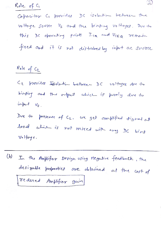
| 100% Q1. (a) A common-emitter amplifier is shown in Figure Q1(a). Explain why the resistor...
Calculate the voltage gain (Av) for the loaded Common Emitter Amplifier below: BAC 200 for all...
 Calculate the voltage gain (Av) for the loaded Common Emitter Amplifier below: BAC 200 for all transistors. Assume re 15 Q for the CE Amplifier. Ignore re' for the DP Amplifier Vcc 12 V, R1 56 K, R2 10 KQ, R4 22 KQ R3 5.6 KQ, RL 8 RE(CE) 628 0, RE(CC) 330 Rc 3.5 KQ, Enter your results. No units. SR3 R1 RC C3 Vcc C1 Beta Q2a HH Vin Beta Q1 Beta Q2b C4 R4 Vs R2 C2...
(10 pts) Consider a common-emitter amplifier with emitter resistor shown below. DC voltage source...
 Common-emitter amplifier?
(10 pts) Consider a common-emitter amplifier with emitter resistor shown below. DC voltage sources VBB and Vcc bias the transistor at lc-1mA. Let β-100. Determine the overall voltage gain Gv 2. VCC 10 k2 Vsig VBB
(10 pts) Consider a common-emitter amplifier with emitter resistor shown below. DC voltage sources VBB and Vcc bias the transistor at lc-1mA. Let β-100. Determine the overall voltage gain Gv 2. VCC 10 k2 Vsig VBB
Common-emitter amplifier?
(10 pts) Consider a common-emitter amplifier with emitter resistor shown below. DC voltage sources VBB and Vcc bias the transistor at lc-1mA. Let β-100. Determine the overall voltage gain Gv 2. VCC 10 k2 Vsig VBB
(10 pts) Consider a common-emitter amplifier with emitter resistor shown below. DC voltage sources VBB and Vcc bias the transistor at lc-1mA. Let β-100. Determine the overall voltage gain Gv 2. VCC 10 k2 Vsig VBB
Question 4: Figure 4 In the series-shunt feedback amplifier shown in Figure 4, the transistors are...
 Question 4: Figure 4 In the series-shunt feedback amplifier shown in Figure 4, the transistors are biased with ideal current-sources 1, 0.1mA, 12 1mA, the devices operate with VE0.7V and t = 100. The input signal V, has a zero DC component. Resistances are (a) If the open loop gain is large, what do you expect the closed-loop gain A, -V/V, to be? Give both an expression and its approximate value (b) Find the DC emitter current in each of...
EEET255 Electronics Page 4 of6 QUESTION 3: [25 marks] Figure 3 shows a feedback amplifier circuit...
 EEET255 Electronics Page 4 of6 QUESTION 3: [25 marks] Figure 3 shows a feedback amplifier circuit R, is the source resistor, R is the feedback resistor and R, is the load resistor. The op-amp has an internal input resistance of R, an intemal output resistance R, and an internal gain of A Apply the "Systematic Analysis" method in this question. Figure 3 3.a State the feedback topology used in the amplifier circuit and which type of feedback amplifier is shown...
Requires 100% correct answer along with pspice 10.24 A transconductance amplifier with negative feedback is shown...
 Requires 100% correct answer along with pspice
10.24 A transconductance amplifier with negative feedback is shown in Fig. P10.24. The amplifier has an open-loop P transconductance of A 50 x 103 A/V, an input resistance of R 25 k!2, and an output resistance of Ro-50 k2. The feedback circuit has RF 2.5 kS2. The source resistance is Rs 1 k, and the load resistance is RL-500 Ω. Determine (a) the input resistance Ri,-vs/is, (b) the output resistance Rof, and (c)...
Requires 100% correct answer along with pspice
10.24 A transconductance amplifier with negative feedback is shown in Fig. P10.24. The amplifier has an open-loop P transconductance of A 50 x 103 A/V, an input resistance of R 25 k!2, and an output resistance of Ro-50 k2. The feedback circuit has RF 2.5 kS2. The source resistance is Rs 1 k, and the load resistance is RL-500 Ω. Determine (a) the input resistance Ri,-vs/is, (b) the output resistance Rof, and (c)...
Figure 2 shows a feedback amplifier circuit. Rs is the source resistor and R, is the...
 Figure 2 shows a feedback amplifier circuit. Rs is the source resistor and R, is the load resistor RS Vs VI RL OPAMP R2 R1 RM R3 R4 Step 1: open-loop and closed-loop circuits identification 1.1 Identify the source, the load, and the closed-loop amplifier 1.2 Identify the open-loop amplifier (**A" eireuit) and the feedback network (B" eircuit) in the closed-loop amplifier 1.3 Identify the connection type between the "A" circuit and the "B" circuit at both the input and...
QUESTION 1 Figure Q1 shows a common emitter (CE) and common Base (CB) cascade amplifier circuit....
 QUESTION 1 Figure Q1 shows a common emitter (CE) and common Base (CB) cascade amplifier circuit. Determine the input and output impedance, Z; and Zo, voltage gain, Avi and Av2 and total cascade voltage gain, Ayr and Ays. [25 marks) 2 +8V 1.5 kn 2.2 F 82 k2 3.3 k2 Vo 2.2 uf B = 100 6.8 k12 1 k 2 what B = 100 tuf ZA 5.6 k 2 47012 ZA V. 33 k2 IuF w 10k_2 -2V w...
100 1.5 0.27 5. 6 Pl. Consider the CB amplifier of Figure 1, for which Vcc-15...
 100 1.5 0.27 5. 6 Pl. Consider the CB amplifier of Figure 1, for which Vcc-15 V, Rs-50 Ω, and RL-10 kQ. For the BJT, assume that B150, VBE.on0.7 V, and VcE,sat 0.3 V, and ignore the Early effect. For the other resistances, however, assume the same values as those you used for the Common-Emitter (CE) amplifier lab (disregard the value for RE2, as the resistor does not exist in the CB amplifier of Figure 1). Therefore, copy the same...
FIND THE VALUES OF Rb1, Rb2, Re,Rc, rin , rout, overall gain and open circuit gain First, design a common emitter BJT a...
 FIND THE VALUES OF Rb1, Rb2, Re,Rc, rin , rout, overall gain and
open circuit gain
First, design a common emitter BJT amplifier Second, analyze the amplifier.( Avo, Gv, Rin, Rout) Third, compare your calculation with Multisim. Report must include comparison between your calculation & simulation results overall voltage gain, open circuit voltage gain, input resistance, and output resistance. This design project is not group work, must be done individually. Type your report. Design a discrete common emitter BJT amplifier.(Determine...
FIND THE VALUES OF Rb1, Rb2, Re,Rc, rin , rout, overall gain and
open circuit gain
First, design a common emitter BJT amplifier Second, analyze the amplifier.( Avo, Gv, Rin, Rout) Third, compare your calculation with Multisim. Report must include comparison between your calculation & simulation results overall voltage gain, open circuit voltage gain, input resistance, and output resistance. This design project is not group work, must be done individually. Type your report. Design a discrete common emitter BJT amplifier.(Determine...
Circuit Analysis The circuit shown in Figure Q3 is a block diagram of an amplifier with...
 Circuit Analysis
The circuit shown in Figure Q3 is a block diagram of an amplifier with a negative feedback. Given that Is 100 uA, IF 99 HA and Vo = 5V. For Figure Q3: (a) Determine the gain without feedback (Ax), gain with feedback (AF) and feedback factor (B), including the units Name the amplifier and feedback topology used. (b) + Zo RL Zi Vo AxIi ZAF ZoF
The circuit shown in Figure Q3 is a block diagram of an...
Circuit Analysis
The circuit shown in Figure Q3 is a block diagram of an amplifier with a negative feedback. Given that Is 100 uA, IF 99 HA and Vo = 5V. For Figure Q3: (a) Determine the gain without feedback (Ax), gain with feedback (AF) and feedback factor (B), including the units Name the amplifier and feedback topology used. (b) + Zo RL Zi Vo AxIi ZAF ZoF
The circuit shown in Figure Q3 is a block diagram of an...
 Calculate the voltage gain (Av) for the loaded Common Emitter Amplifier below: BAC 200 for all transistors. Assume re 15 Q for the CE Amplifier. Ignore re' for the DP Amplifier Vcc 12 V, R1 56 K, R2 10 KQ, R4 22 KQ R3 5.6 KQ, RL 8 RE(CE) 628 0, RE(CC) 330 Rc 3.5 KQ, Enter your results. No units. SR3 R1 RC C3 Vcc C1 Beta Q2a HH Vin Beta Q1 Beta Q2b C4 R4 Vs R2 C2...
 Common-emitter amplifier?
(10 pts) Consider a common-emitter amplifier with emitter resistor shown below. DC voltage sources VBB and Vcc bias the transistor at lc-1mA. Let β-100. Determine the overall voltage gain Gv 2. VCC 10 k2 Vsig VBB
(10 pts) Consider a common-emitter amplifier with emitter resistor shown below. DC voltage sources VBB and Vcc bias the transistor at lc-1mA. Let β-100. Determine the overall voltage gain Gv 2. VCC 10 k2 Vsig VBB
Common-emitter amplifier?
(10 pts) Consider a common-emitter amplifier with emitter resistor shown below. DC voltage sources VBB and Vcc bias the transistor at lc-1mA. Let β-100. Determine the overall voltage gain Gv 2. VCC 10 k2 Vsig VBB
(10 pts) Consider a common-emitter amplifier with emitter resistor shown below. DC voltage sources VBB and Vcc bias the transistor at lc-1mA. Let β-100. Determine the overall voltage gain Gv 2. VCC 10 k2 Vsig VBB
 Question 4: Figure 4 In the series-shunt feedback amplifier shown in Figure 4, the transistors are biased with ideal current-sources 1, 0.1mA, 12 1mA, the devices operate with VE0.7V and t = 100. The input signal V, has a zero DC component. Resistances are (a) If the open loop gain is large, what do you expect the closed-loop gain A, -V/V, to be? Give both an expression and its approximate value (b) Find the DC emitter current in each of...
 EEET255 Electronics Page 4 of6 QUESTION 3: [25 marks] Figure 3 shows a feedback amplifier circuit R, is the source resistor, R is the feedback resistor and R, is the load resistor. The op-amp has an internal input resistance of R, an intemal output resistance R, and an internal gain of A Apply the "Systematic Analysis" method in this question. Figure 3 3.a State the feedback topology used in the amplifier circuit and which type of feedback amplifier is shown...
 Requires 100% correct answer along with pspice
10.24 A transconductance amplifier with negative feedback is shown in Fig. P10.24. The amplifier has an open-loop P transconductance of A 50 x 103 A/V, an input resistance of R 25 k!2, and an output resistance of Ro-50 k2. The feedback circuit has RF 2.5 kS2. The source resistance is Rs 1 k, and the load resistance is RL-500 Ω. Determine (a) the input resistance Ri,-vs/is, (b) the output resistance Rof, and (c)...
Requires 100% correct answer along with pspice
10.24 A transconductance amplifier with negative feedback is shown in Fig. P10.24. The amplifier has an open-loop P transconductance of A 50 x 103 A/V, an input resistance of R 25 k!2, and an output resistance of Ro-50 k2. The feedback circuit has RF 2.5 kS2. The source resistance is Rs 1 k, and the load resistance is RL-500 Ω. Determine (a) the input resistance Ri,-vs/is, (b) the output resistance Rof, and (c)...
 Figure 2 shows a feedback amplifier circuit. Rs is the source resistor and R, is the load resistor RS Vs VI RL OPAMP R2 R1 RM R3 R4 Step 1: open-loop and closed-loop circuits identification 1.1 Identify the source, the load, and the closed-loop amplifier 1.2 Identify the open-loop amplifier (**A" eireuit) and the feedback network (B" eircuit) in the closed-loop amplifier 1.3 Identify the connection type between the "A" circuit and the "B" circuit at both the input and...
 QUESTION 1 Figure Q1 shows a common emitter (CE) and common Base (CB) cascade amplifier circuit. Determine the input and output impedance, Z; and Zo, voltage gain, Avi and Av2 and total cascade voltage gain, Ayr and Ays. [25 marks) 2 +8V 1.5 kn 2.2 F 82 k2 3.3 k2 Vo 2.2 uf B = 100 6.8 k12 1 k 2 what B = 100 tuf ZA 5.6 k 2 47012 ZA V. 33 k2 IuF w 10k_2 -2V w...
 100 1.5 0.27 5. 6 Pl. Consider the CB amplifier of Figure 1, for which Vcc-15 V, Rs-50 Ω, and RL-10 kQ. For the BJT, assume that B150, VBE.on0.7 V, and VcE,sat 0.3 V, and ignore the Early effect. For the other resistances, however, assume the same values as those you used for the Common-Emitter (CE) amplifier lab (disregard the value for RE2, as the resistor does not exist in the CB amplifier of Figure 1). Therefore, copy the same...
 FIND THE VALUES OF Rb1, Rb2, Re,Rc, rin , rout, overall gain and
open circuit gain
First, design a common emitter BJT amplifier Second, analyze the amplifier.( Avo, Gv, Rin, Rout) Third, compare your calculation with Multisim. Report must include comparison between your calculation & simulation results overall voltage gain, open circuit voltage gain, input resistance, and output resistance. This design project is not group work, must be done individually. Type your report. Design a discrete common emitter BJT amplifier.(Determine...
FIND THE VALUES OF Rb1, Rb2, Re,Rc, rin , rout, overall gain and
open circuit gain
First, design a common emitter BJT amplifier Second, analyze the amplifier.( Avo, Gv, Rin, Rout) Third, compare your calculation with Multisim. Report must include comparison between your calculation & simulation results overall voltage gain, open circuit voltage gain, input resistance, and output resistance. This design project is not group work, must be done individually. Type your report. Design a discrete common emitter BJT amplifier.(Determine...
 Circuit Analysis
The circuit shown in Figure Q3 is a block diagram of an amplifier with a negative feedback. Given that Is 100 uA, IF 99 HA and Vo = 5V. For Figure Q3: (a) Determine the gain without feedback (Ax), gain with feedback (AF) and feedback factor (B), including the units Name the amplifier and feedback topology used. (b) + Zo RL Zi Vo AxIi ZAF ZoF
The circuit shown in Figure Q3 is a block diagram of an...
Circuit Analysis
The circuit shown in Figure Q3 is a block diagram of an amplifier with a negative feedback. Given that Is 100 uA, IF 99 HA and Vo = 5V. For Figure Q3: (a) Determine the gain without feedback (Ax), gain with feedback (AF) and feedback factor (B), including the units Name the amplifier and feedback topology used. (b) + Zo RL Zi Vo AxIi ZAF ZoF
The circuit shown in Figure Q3 is a block diagram of an...
Most questions answered within 3 hours.
-
1-The Electrons in a beam are moving at 2.7×10⁸ m/s in an
electric field of 15000...
asked 2 minutes ago -
A gas tank is a vertical cylinder. It has a radius of 1m, a
height of...
asked 28 minutes ago -
Accent Software faces the following conditions. All of these
support Accent’s use of a market-penetration pricing...
asked 1 hour ago -
A mathematically inclined friend emails you the following
instructions: "Meet me in the cafeteria the first...
asked 1 hour ago -
A monopoly sells in two countries . The demand curves in the two
countries are p1...
asked 2 hours ago -
A .15kg rubber ball is bounced off a wall. Before hitting the
wall, the ball moves...
asked 3 hours ago -
A manufacturing company preparing to build a new plant is
considering three potential locations for it....
asked 3 hours ago -
B. If compound Y has approximately the same values of solubility
in toluene as compound X,...
asked 3 hours ago -
Oscar Inc. has inventory in Japan valued at 39,051,000 Yen one
year ago. One year ago...
asked 4 hours ago -
If Canada suffered from "fundamental disequilibrium," and its
government choose not to devalue its currency, a...
asked 4 hours ago -
4. How many input & output Key Value Pairs are passed into,
and emitted out of...
asked 4 hours ago -
Why would your heart not function well if constructed of
skeletal muscle? What is the particular...
asked 4 hours ago