![EEET255 Electronics Page 4 of6 QUESTION 3: [25 marks] Figure 3 shows a feedback amplifier circuit R, is the source resistor,](http://img.homeworklib.com/images/58c36b05-caa0-4523-a0d0-1c071c730ff2.png?x-oss-process=image/resize,w_560)
Homework Answers


 if you have any questions
please comment below and in the given problem rout means rof and
rin means rif just I calculate by analuanal the shunt mixing
network . please upvote thanks
if you have any questions
please comment below and in the given problem rout means rof and
rin means rif just I calculate by analuanal the shunt mixing
network . please upvote thanks
Add Answer to:
EEET255 Electronics Page 4 of6 QUESTION 3: [25 marks] Figure 3 shows a feedback amplifier circuit...
Question 4: Figure 4 In the series-shunt feedback amplifier shown in Figure 4, the transistors are...
 Question 4: Figure 4 In the series-shunt feedback amplifier shown in Figure 4, the transistors are biased with ideal current-sources 1, 0.1mA, 12 1mA, the devices operate with VE0.7V and t = 100. The input signal V, has a zero DC component. Resistances are (a) If the open loop gain is large, what do you expect the closed-loop gain A, -V/V, to be? Give both an expression and its approximate value (b) Find the DC emitter current in each of...
Figure 2 shows a feedback amplifier circuit. Rs is the source resistor and R, is the...
 Figure 2 shows a feedback amplifier circuit. Rs is the source resistor and R, is the load resistor RS Vs VI RL OPAMP R2 R1 RM R3 R4 Step 1: open-loop and closed-loop circuits identification 1.1 Identify the source, the load, and the closed-loop amplifier 1.2 Identify the open-loop amplifier (**A" eireuit) and the feedback network (B" eircuit) in the closed-loop amplifier 1.3 Identify the connection type between the "A" circuit and the "B" circuit at both the input and...
Problem 2 Consider the feedback amplifier circuit on Figure P2. The DC current gain of transistor Q3 is -100 1. What type of feedback (or what feedback topology) do we have on the circuit in Figure P...
 Problem 2 Consider the feedback amplifier circuit on Figure P2. The DC current gain of transistor Q3 is -100 1. What type of feedback (or what feedback topology) do we have on the circuit in Figure P2? 2. Draw the A-circuit. Express and compute the open-loop voltage gain A at mid-band frequency 3, Draw the γ-circuit. Express and compute the feedback factor γ 4. Express and compute the overall gain of the feedback amplifier Ap Express and compute the input...
Question 1 (10 marks) Figure 10 Rc2 shunt-shunt28R feedback amplifier circuit The resistors values and the transistors parameters are also indicated in Figure 1 1,-0.3mA 285m Hint: in DC analysis...
 Question 1 (10 marks) Figure 10 Rc2 shunt-shunt28R feedback amplifier circuit The resistors values and the transistors parameters are also indicated in Figure 1 1,-0.3mA 285m Hint: in DC analysis; 1) For R,-104, determine the small-signal closed-loop current-gain'. 2) Determine the small-signal open-loop current-gain 3) From the results of 2) and 3), determine the loop-gain T: Hint: If you did not solve 2), assume If you did not solve 3), assume600
Question 1 (10 marks) Figure 10 Rc2 shunt-shunt28R feedback...
Question 1 (10 marks) Figure 10 Rc2 shunt-shunt28R feedback amplifier circuit The resistors values and the transistors parameters are also indicated in Figure 1 1,-0.3mA 285m Hint: in DC analysis; 1) For R,-104, determine the small-signal closed-loop current-gain'. 2) Determine the small-signal open-loop current-gain 3) From the results of 2) and 3), determine the loop-gain T: Hint: If you did not solve 2), assume If you did not solve 3), assume600
Question 1 (10 marks) Figure 10 Rc2 shunt-shunt28R feedback...
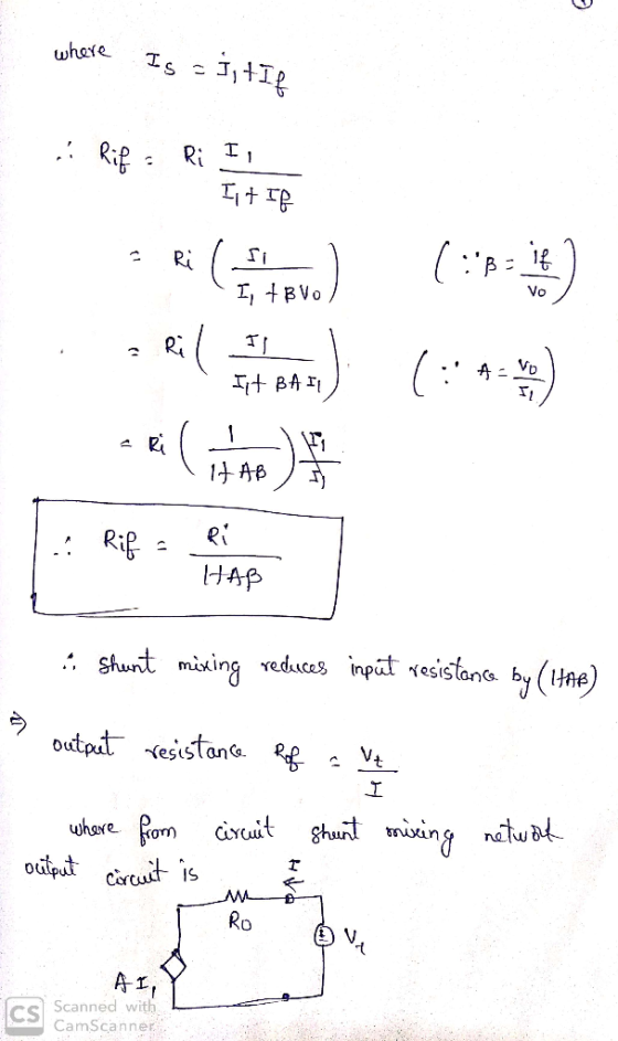
Find the induction process of A, β, Ro, Ri. EXAMPLE 10.10 Figure 10.27 shows a feedback current amplifier formed by cas...
 Find the induction process of A, β, Ro, Ri.
EXAMPLE 10.10 Figure 10.27 shows a feedback current amplifier formed by cascading an inverting voltage amplifier u witha MOSFET Q. The output current I, is the drain current of Q. The feedback network, consisting of resistors R, and R, senses an exactly equal current, namely, the source current of Q, and provides feedback current signal that is mixed with I, at the input node. Note that the bias arrangement is not...
Find the induction process of A, β, Ro, Ri.
EXAMPLE 10.10 Figure 10.27 shows a feedback current amplifier formed by cascading an inverting voltage amplifier u witha MOSFET Q. The output current I, is the drain current of Q. The feedback network, consisting of resistors R, and R, senses an exactly equal current, namely, the source current of Q, and provides feedback current signal that is mixed with I, at the input node. Note that the bias arrangement is not...
The transistor in Figure 4 is biased so that Ic 10mA and VcE 6V. The transistor...
 The transistor in Figure 4 is biased so that Ic 10mA and VcE 6V. The transistor parameters are: B -150 and VA 120V. Vcc 12V Rc 596 vout Rf 79.5k 01 C2 Rs 1Meg 1uA in Figure 4 BJT feedback amplifier (a) Sketch the feedback circuit and identify the type of feedback. (b) What type of amplifier is this? (c) Calculate the feedback factor (d) Sketch the open loop small signal equivalent circuit. (e) Calculate the open loop gain (f)...
Q 3. The depletion NMOS amplifier of Figure 2 has R,-50052. RL-10kS2. RSR-RD-5kS2. RG-100kS2. IDD...
 Q 3. The depletion NMOS amplifier of Figure 2 has R,-50052. RL-10kS2. RSR-RD-5kS2. RG-100kS2. IDD 10mA.Vp4V, |VMl 200V, and VDD 12V. Calculate (a) the input resistance Rin /i, (b) the no-load voltage gain Avo-Vo/Vy, (c) the output resistance Ro , and (d) the overall voltage gain A,-uz/vs. RD SR out Figure 2
Q 3. The depletion NMOS amplifier of Figure 2 has R,-50052. RL-10kS2. RSR-RD-5kS2. RG-100kS2. IDD 10mA.Vp4V, |VMl 200V, and VDD 12V. Calculate (a) the input resistance Rin /i,...
Q 3. The depletion NMOS amplifier of Figure 2 has R,-50052. RL-10kS2. RSR-RD-5kS2. RG-100kS2. IDD 10mA.Vp4V, |VMl 200V, and VDD 12V. Calculate (a) the input resistance Rin /i, (b) the no-load voltage gain Avo-Vo/Vy, (c) the output resistance Ro , and (d) the overall voltage gain A,-uz/vs. RD SR out Figure 2
Q 3. The depletion NMOS amplifier of Figure 2 has R,-50052. RL-10kS2. RSR-RD-5kS2. RG-100kS2. IDD 10mA.Vp4V, |VMl 200V, and VDD 12V. Calculate (a) the input resistance Rin /i,...
Question1 Figure 1 represents a shunt-shunt feedback amplifier circuit. The resistors' values and the transistors parameters are also indicated in Figure 1 Voo 8100 Rci 28 KS2 Rci D10 | R.-S...
 Question1 Figure 1 represents a shunt-shunt feedback amplifier circuit. The resistors' values and the transistors parameters are also indicated in Figure 1 Voo 8100 Rci 28 KS2 Rci D10 | R.-S㏀ Hint: in DC analysis; gl -11.538mA/V and 0 R0.2k2 822.85mA/V IE 0.3mA Figure- 1) For R, -10 k2, determine the small-signal closed-loop current-gain A, 2) Determine the small-signal open-loop current-gain.4,- 3) From the results of 2) and 3), determine the loop-gain T Kint: If you did not solve a),...
Requires 100% correct answer along with pspice 10.24 A transconductance amplifier with negative feedback is shown...
 Requires 100% correct answer along with pspice
10.24 A transconductance amplifier with negative feedback is shown in Fig. P10.24. The amplifier has an open-loop P transconductance of A 50 x 103 A/V, an input resistance of R 25 k!2, and an output resistance of Ro-50 k2. The feedback circuit has RF 2.5 kS2. The source resistance is Rs 1 k, and the load resistance is RL-500 Ω. Determine (a) the input resistance Ri,-vs/is, (b) the output resistance Rof, and (c)...
Requires 100% correct answer along with pspice
10.24 A transconductance amplifier with negative feedback is shown in Fig. P10.24. The amplifier has an open-loop P transconductance of A 50 x 103 A/V, an input resistance of R 25 k!2, and an output resistance of Ro-50 k2. The feedback circuit has RF 2.5 kS2. The source resistance is Rs 1 k, and the load resistance is RL-500 Ω. Determine (a) the input resistance Ri,-vs/is, (b) the output resistance Rof, and (c)...
4. For the amplifier in the figure below use the parameters in the table: +Vcc Re VBE- 0.7V, Ri- ...
 4. For the amplifier in the figure below use the parameters in the table: +Vcc Re VBE- 0.7V, Ri- 1002, R1-160k2, R2-320k2 R3-200k2, R6-40 k2, Rc-60k2, Vcc- 12V, Ry Do a) Draw the DC equivalent circuit and calculate the Q-point. c) Draw the AC equivalent circuit with the small signal model for the transistor. d) Calculate the voltage gain, Av-Vo/vi. Assume ro infinite. e) Draw the circuit to find the amplifier input resistance (Rin). Calculate Rin f Draw the circuit...
 Question 4: Figure 4 In the series-shunt feedback amplifier shown in Figure 4, the transistors are biased with ideal current-sources 1, 0.1mA, 12 1mA, the devices operate with VE0.7V and t = 100. The input signal V, has a zero DC component. Resistances are (a) If the open loop gain is large, what do you expect the closed-loop gain A, -V/V, to be? Give both an expression and its approximate value (b) Find the DC emitter current in each of...
 Figure 2 shows a feedback amplifier circuit. Rs is the source resistor and R, is the load resistor RS Vs VI RL OPAMP R2 R1 RM R3 R4 Step 1: open-loop and closed-loop circuits identification 1.1 Identify the source, the load, and the closed-loop amplifier 1.2 Identify the open-loop amplifier (**A" eireuit) and the feedback network (B" eircuit) in the closed-loop amplifier 1.3 Identify the connection type between the "A" circuit and the "B" circuit at both the input and...
 Problem 2 Consider the feedback amplifier circuit on Figure P2. The DC current gain of transistor Q3 is -100 1. What type of feedback (or what feedback topology) do we have on the circuit in Figure P2? 2. Draw the A-circuit. Express and compute the open-loop voltage gain A at mid-band frequency 3, Draw the γ-circuit. Express and compute the feedback factor γ 4. Express and compute the overall gain of the feedback amplifier Ap Express and compute the input...
 Question 1 (10 marks) Figure 10 Rc2 shunt-shunt28R feedback amplifier circuit The resistors values and the transistors parameters are also indicated in Figure 1 1,-0.3mA 285m Hint: in DC analysis; 1) For R,-104, determine the small-signal closed-loop current-gain'. 2) Determine the small-signal open-loop current-gain 3) From the results of 2) and 3), determine the loop-gain T: Hint: If you did not solve 2), assume If you did not solve 3), assume600
Question 1 (10 marks) Figure 10 Rc2 shunt-shunt28R feedback...
Question 1 (10 marks) Figure 10 Rc2 shunt-shunt28R feedback amplifier circuit The resistors values and the transistors parameters are also indicated in Figure 1 1,-0.3mA 285m Hint: in DC analysis; 1) For R,-104, determine the small-signal closed-loop current-gain'. 2) Determine the small-signal open-loop current-gain 3) From the results of 2) and 3), determine the loop-gain T: Hint: If you did not solve 2), assume If you did not solve 3), assume600
Question 1 (10 marks) Figure 10 Rc2 shunt-shunt28R feedback...
 Find the induction process of A, β, Ro, Ri.
EXAMPLE 10.10 Figure 10.27 shows a feedback current amplifier formed by cascading an inverting voltage amplifier u witha MOSFET Q. The output current I, is the drain current of Q. The feedback network, consisting of resistors R, and R, senses an exactly equal current, namely, the source current of Q, and provides feedback current signal that is mixed with I, at the input node. Note that the bias arrangement is not...
Find the induction process of A, β, Ro, Ri.
EXAMPLE 10.10 Figure 10.27 shows a feedback current amplifier formed by cascading an inverting voltage amplifier u witha MOSFET Q. The output current I, is the drain current of Q. The feedback network, consisting of resistors R, and R, senses an exactly equal current, namely, the source current of Q, and provides feedback current signal that is mixed with I, at the input node. Note that the bias arrangement is not...
 The transistor in Figure 4 is biased so that Ic 10mA and VcE 6V. The transistor parameters are: B -150 and VA 120V. Vcc 12V Rc 596 vout Rf 79.5k 01 C2 Rs 1Meg 1uA in Figure 4 BJT feedback amplifier (a) Sketch the feedback circuit and identify the type of feedback. (b) What type of amplifier is this? (c) Calculate the feedback factor (d) Sketch the open loop small signal equivalent circuit. (e) Calculate the open loop gain (f)...
 Q 3. The depletion NMOS amplifier of Figure 2 has R,-50052. RL-10kS2. RSR-RD-5kS2. RG-100kS2. IDD 10mA.Vp4V, |VMl 200V, and VDD 12V. Calculate (a) the input resistance Rin /i, (b) the no-load voltage gain Avo-Vo/Vy, (c) the output resistance Ro , and (d) the overall voltage gain A,-uz/vs. RD SR out Figure 2
Q 3. The depletion NMOS amplifier of Figure 2 has R,-50052. RL-10kS2. RSR-RD-5kS2. RG-100kS2. IDD 10mA.Vp4V, |VMl 200V, and VDD 12V. Calculate (a) the input resistance Rin /i,...
Q 3. The depletion NMOS amplifier of Figure 2 has R,-50052. RL-10kS2. RSR-RD-5kS2. RG-100kS2. IDD 10mA.Vp4V, |VMl 200V, and VDD 12V. Calculate (a) the input resistance Rin /i, (b) the no-load voltage gain Avo-Vo/Vy, (c) the output resistance Ro , and (d) the overall voltage gain A,-uz/vs. RD SR out Figure 2
Q 3. The depletion NMOS amplifier of Figure 2 has R,-50052. RL-10kS2. RSR-RD-5kS2. RG-100kS2. IDD 10mA.Vp4V, |VMl 200V, and VDD 12V. Calculate (a) the input resistance Rin /i,...
 Question1 Figure 1 represents a shunt-shunt feedback amplifier circuit. The resistors' values and the transistors parameters are also indicated in Figure 1 Voo 8100 Rci 28 KS2 Rci D10 | R.-S㏀ Hint: in DC analysis; gl -11.538mA/V and 0 R0.2k2 822.85mA/V IE 0.3mA Figure- 1) For R, -10 k2, determine the small-signal closed-loop current-gain A, 2) Determine the small-signal open-loop current-gain.4,- 3) From the results of 2) and 3), determine the loop-gain T Kint: If you did not solve a),...
 Requires 100% correct answer along with pspice
10.24 A transconductance amplifier with negative feedback is shown in Fig. P10.24. The amplifier has an open-loop P transconductance of A 50 x 103 A/V, an input resistance of R 25 k!2, and an output resistance of Ro-50 k2. The feedback circuit has RF 2.5 kS2. The source resistance is Rs 1 k, and the load resistance is RL-500 Ω. Determine (a) the input resistance Ri,-vs/is, (b) the output resistance Rof, and (c)...
Requires 100% correct answer along with pspice
10.24 A transconductance amplifier with negative feedback is shown in Fig. P10.24. The amplifier has an open-loop P transconductance of A 50 x 103 A/V, an input resistance of R 25 k!2, and an output resistance of Ro-50 k2. The feedback circuit has RF 2.5 kS2. The source resistance is Rs 1 k, and the load resistance is RL-500 Ω. Determine (a) the input resistance Ri,-vs/is, (b) the output resistance Rof, and (c)...
 4. For the amplifier in the figure below use the parameters in the table: +Vcc Re VBE- 0.7V, Ri- 1002, R1-160k2, R2-320k2 R3-200k2, R6-40 k2, Rc-60k2, Vcc- 12V, Ry Do a) Draw the DC equivalent circuit and calculate the Q-point. c) Draw the AC equivalent circuit with the small signal model for the transistor. d) Calculate the voltage gain, Av-Vo/vi. Assume ro infinite. e) Draw the circuit to find the amplifier input resistance (Rin). Calculate Rin f Draw the circuit...
Most questions answered within 3 hours.
-
Consider the reaction, C3 H8 + O2 --> CO2 + H2O. How many
moles of O2...
asked 1 hour ago -
You and your opponent both roll a fair die. If you both roll the
same number,...
asked 1 hour ago -
In a study of the accuracy of fast food drive-through orders,
Restaurant A had 257 accurate...
asked 1 hour ago -
Identify and describe in detail the four categories of
institutions that could be included in a...
asked 1 hour ago -
In python
class Customer:
def __init__(self, customer_id, last_name, first_name, phone_number, address):
self._customer_id = int(customer_id)
self._last_name =...
asked 1 hour ago -
What is an example of a limitation in implementing a new
ERP system and how it...
asked 1 hour ago -
In a section of 9.7cm of an artery with a radius of 2.6mm there
is a...
asked 1 hour ago -
the two carboxylic acid groups of aspartic acid have different
acidities with pKa values of 2.1...
asked 1 hour ago -
Would CuCO3 aqueous salt combined with calcium chloride
form a solid precipitate? If so, what would...
asked 1 hour ago -
How do ECM Solutions assist in embedding a culture of continuous
improvement in an organization? (Project...
asked 1 hour ago -
Directions
These directions introduce the idea of Essential Questions.
Since this may be a new concept...
asked 1 hour ago -
1.b. Fiscal policy is said to suffer from ‘crowding out’.
Explain what this means and why...
asked 2 hours ago