
Homework Answers


![5) For! B-150 from einn I B = VB to 7 RB+(B+1)RE ~3. 37 IBE 3.2K+ (15102kn In a IB=-3-31 = -0.098mA - 33.4kn TT B=-0.098mA] I](http://img.homeworklib.com/questions/0b094ee0-4ada-11eb-82eb-df0c12b97a27.png?x-oss-process=image/resize,w_560)
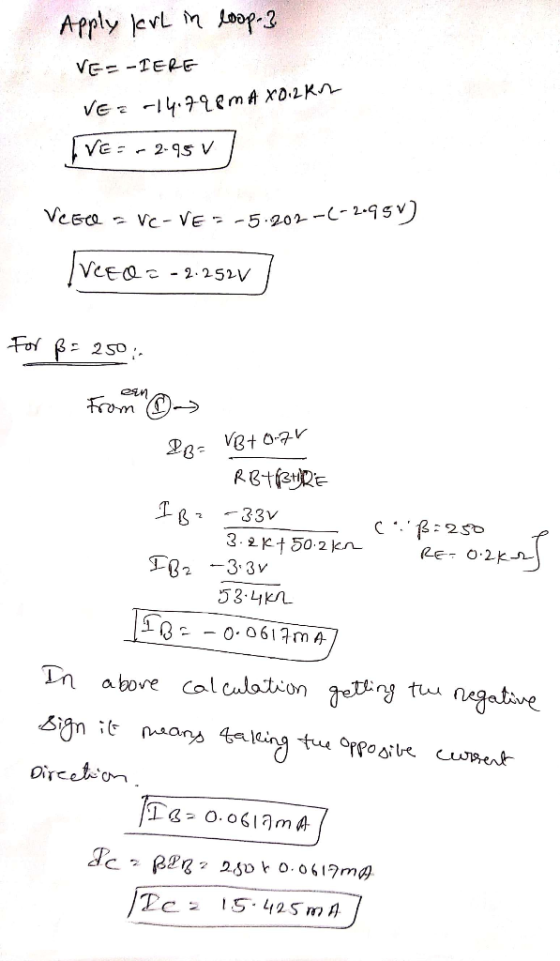
![AIE = (+1) FB 251* 0.06171 SEZ 15.486 Энерlу ем іn dое - ve Ic Rc-Vcc=0 Vc=ICRetree VC= 15.425x1 - 20 [re=r4.5750] - Apply Kv](http://img.homeworklib.com/questions/0c352e20-4ada-11eb-b81d-1103bb355e94.png?x-oss-process=image/resize,w_560)

Add Answer to:
4. For the emitter-resistor amplifier with a voltage divider bias configuration using a single source as...
ASSUME ALL CAPACITORS ARE INFINITE AND IDEAL. For a common-emitter amplifier with a voltage divider bias...
 ASSUME ALL CAPACITORS ARE INFINITE
AND IDEAL.
For a common-emitter amplifier with a voltage divider bias configuration using a single source, and given Rs = 2009, Rc = R = 2k2, VBE = 0.7V, Vcc= 20V and B = 100: a. Find R. and R for maximum symmetric output swing b. Determine Vopp (ideal and practical) c. Sketch the dc and ac load lines, showing the q-point and all intercept values of voltage and current.
ASSUME ALL CAPACITORS ARE INFINITE
AND IDEAL.
For a common-emitter amplifier with a voltage divider bias configuration using a single source, and given Rs = 2009, Rc = R = 2k2, VBE = 0.7V, Vcc= 20V and B = 100: a. Find R. and R for maximum symmetric output swing b. Determine Vopp (ideal and practical) c. Sketch the dc and ac load lines, showing the q-point and all intercept values of voltage and current.
5. Determine the Ico and Vceo for the emitter-biased common-emitter amplifier circuit show below. Assume B=180....
 5. Determine the Ico and Vceo for the emitter-biased common-emitter amplifier circuit show below. Assume B=180. (12 points) Vcc 918 v Rs12330 ks Rc 1,5 k22 Rs2 B V ce 18 220 ke2 RE 30.75 k2 6. Draw the circuit diagram of a common-emitter voltage-divider bias with the following parameters. (12 points) Vcc = 16V, R, -30k1, R2 = 10k22, Rc = 3.3kQ2, Re = 1.5k22, B = 199 (a) Determine lco and Vcro using the approximate method. (b) Determine...
(10 pts) Consider a common-emitter amplifier with emitter resistor shown below. DC voltage source...
 Common-emitter amplifier?
(10 pts) Consider a common-emitter amplifier with emitter resistor shown below. DC voltage sources VBB and Vcc bias the transistor at lc-1mA. Let β-100. Determine the overall voltage gain Gv 2. VCC 10 k2 Vsig VBB
(10 pts) Consider a common-emitter amplifier with emitter resistor shown below. DC voltage sources VBB and Vcc bias the transistor at lc-1mA. Let β-100. Determine the overall voltage gain Gv 2. VCC 10 k2 Vsig VBB
Common-emitter amplifier?
(10 pts) Consider a common-emitter amplifier with emitter resistor shown below. DC voltage sources VBB and Vcc bias the transistor at lc-1mA. Let β-100. Determine the overall voltage gain Gv 2. VCC 10 k2 Vsig VBB
(10 pts) Consider a common-emitter amplifier with emitter resistor shown below. DC voltage sources VBB and Vcc bias the transistor at lc-1mA. Let β-100. Determine the overall voltage gain Gv 2. VCC 10 k2 Vsig VBB
In a small signal voltage amplifier using a pnp transistor shown below, the voltage gain is 350.2. The value of a-0.95. Find the equivalent model emitter resistance re in Ohms if Rc-4.1K2. The BJT is...
 In a small signal voltage amplifier using a pnp transistor shown below, the voltage gain is 350.2. The value of a-0.95. Find the equivalent model emitter resistance re in Ohms if Rc-4.1K2. The BJT is operating at room temperature and VBE 0.7V RE-10K CCI vi Cc2 Rc
In a small signal voltage amplifier using a pnp transistor shown below, the voltage gain is 350.2. The value of a-0.95. Find the equivalent model emitter resistance re in Ohms if Rc-4.1K2. The...
In a small signal voltage amplifier using a pnp transistor shown below, the voltage gain is 350.2. The value of a-0.95. Find the equivalent model emitter resistance re in Ohms if Rc-4.1K2. The BJT is operating at room temperature and VBE 0.7V RE-10K CCI vi Cc2 Rc
In a small signal voltage amplifier using a pnp transistor shown below, the voltage gain is 350.2. The value of a-0.95. Find the equivalent model emitter resistance re in Ohms if Rc-4.1K2. The...
8. Design the DC bias circuit of a voltage-divider biased common-emitter amplifier (12 points) with the...
 8. Design the DC bias circuit of a voltage-divider biased common-emitter amplifier (12 points) with the specification given below. Center Q-point, Vcc- 16V, Ico-2.2mA.
Perform a simple initial design of an ac coupled common-emitter amplifier with four resistor biasing and emitter by-pass...
 Perform a simple initial design of an ac coupled common-emitter
amplifier with
four resistor biasing and emitter by-pass capacitor, to have a
voltage gain of about
100, for the following conditions. Justify any approximations used.
(Assume Ic=1/300 A)
i)Transistor ac common-emitter gain, B, 100 ii) Supply voltage ofV0c-20V iii) Allow 10% Vcc across RE DC collector voltage of 10 V iv) v) DC current in the base bias resistors should be ten times greater than the DC base current. Assume...
Perform a simple initial design of an ac coupled common-emitter
amplifier with
four resistor biasing and emitter by-pass capacitor, to have a
voltage gain of about
100, for the following conditions. Justify any approximations used.
(Assume Ic=1/300 A)
i)Transistor ac common-emitter gain, B, 100 ii) Supply voltage ofV0c-20V iii) Allow 10% Vcc across RE DC collector voltage of 10 V iv) v) DC current in the base bias resistors should be ten times greater than the DC base current. Assume...
3.1. For the BJT differential pair configuration shown below, assume the input transistor beta is very large. Then...
 3.1. For the BJT differential pair configuration shown below,
assume the input transistor beta is very large.
Then find the differential signal vd = vB1 − vB2 sufficient to
cause:
3.2. A differential amplifier resembling that below uses I =
200μA, RC = 10kohm and VCC = 3V. Assume beta is very large
3.4.For the emitter follower in the figure below, given VCC =
15 V, VEE = −15 V, RL = 1 kohm and beta = 100 for all...
3.1. For the BJT differential pair configuration shown below,
assume the input transistor beta is very large.
Then find the differential signal vd = vB1 − vB2 sufficient to
cause:
3.2. A differential amplifier resembling that below uses I =
200μA, RC = 10kohm and VCC = 3V. Assume beta is very large
3.4.For the emitter follower in the figure below, given VCC =
15 V, VEE = −15 V, RL = 1 kohm and beta = 100 for all...
Design a BJT amplifier based on the specifications provided in the table below. Your design shoul...
 THE STEPS TO DO SO:
Design a BJT amplifier based on the specifications provided in the table below. Your design should be insensitive to β variations, and both the input and the output should be AC coupled as in Fig. 1. Supply Voltage, Vcc Load Resistance, RL Transistor's Current Gain, β Relative Variation of lc for VBE-0.7 ± 0.1 V 0-to-Peak Output Swing, Vo Voltage Gain, A Input Resistance, R THD for 5kHz IV (0-to-peak) Sine Wave Output Voltage, V。S5%...
THE STEPS TO DO SO:
Design a BJT amplifier based on the specifications provided in the table below. Your design should be insensitive to β variations, and both the input and the output should be AC coupled as in Fig. 1. Supply Voltage, Vcc Load Resistance, RL Transistor's Current Gain, β Relative Variation of lc for VBE-0.7 ± 0.1 V 0-to-Peak Output Swing, Vo Voltage Gain, A Input Resistance, R THD for 5kHz IV (0-to-peak) Sine Wave Output Voltage, V。S5%...
1.0 kn. RE-390 Ω, r-15 Ω. and ßac-75. 5. For a common-emitter amplifier, Rc Assuming that Rg is completely bypassed at the operating frequency, the voltage gain is (a) 66.7 (d) 75 (b) 2.56 (c) 2....
 1.0 kn. RE-390 Ω, r-15 Ω. and ßac-75. 5. For a common-emitter amplifier, Rc Assuming that Rg is completely bypassed at the operating frequency, the voltage gain is (a) 66.7 (d) 75 (b) 2.56 (c) 2.47 6. In the circuit of Question 5, if the frequency is reduced to the point where Xctbypass) RE, the voltage gain (a) remains the same (b) is less (c) is greater 7. In a common-emitter amplifier with voltage-divider bias, Rimlbase) 68 k2, Ri 33...
 ASSUME ALL CAPACITORS ARE INFINITE
AND IDEAL.
For a common-emitter amplifier with a voltage divider bias configuration using a single source, and given Rs = 2009, Rc = R = 2k2, VBE = 0.7V, Vcc= 20V and B = 100: a. Find R. and R for maximum symmetric output swing b. Determine Vopp (ideal and practical) c. Sketch the dc and ac load lines, showing the q-point and all intercept values of voltage and current.
ASSUME ALL CAPACITORS ARE INFINITE
AND IDEAL.
For a common-emitter amplifier with a voltage divider bias configuration using a single source, and given Rs = 2009, Rc = R = 2k2, VBE = 0.7V, Vcc= 20V and B = 100: a. Find R. and R for maximum symmetric output swing b. Determine Vopp (ideal and practical) c. Sketch the dc and ac load lines, showing the q-point and all intercept values of voltage and current.
 5. Determine the Ico and Vceo for the emitter-biased common-emitter amplifier circuit show below. Assume B=180. (12 points) Vcc 918 v Rs12330 ks Rc 1,5 k22 Rs2 B V ce 18 220 ke2 RE 30.75 k2 6. Draw the circuit diagram of a common-emitter voltage-divider bias with the following parameters. (12 points) Vcc = 16V, R, -30k1, R2 = 10k22, Rc = 3.3kQ2, Re = 1.5k22, B = 199 (a) Determine lco and Vcro using the approximate method. (b) Determine...
 Common-emitter amplifier?
(10 pts) Consider a common-emitter amplifier with emitter resistor shown below. DC voltage sources VBB and Vcc bias the transistor at lc-1mA. Let β-100. Determine the overall voltage gain Gv 2. VCC 10 k2 Vsig VBB
(10 pts) Consider a common-emitter amplifier with emitter resistor shown below. DC voltage sources VBB and Vcc bias the transistor at lc-1mA. Let β-100. Determine the overall voltage gain Gv 2. VCC 10 k2 Vsig VBB
Common-emitter amplifier?
(10 pts) Consider a common-emitter amplifier with emitter resistor shown below. DC voltage sources VBB and Vcc bias the transistor at lc-1mA. Let β-100. Determine the overall voltage gain Gv 2. VCC 10 k2 Vsig VBB
(10 pts) Consider a common-emitter amplifier with emitter resistor shown below. DC voltage sources VBB and Vcc bias the transistor at lc-1mA. Let β-100. Determine the overall voltage gain Gv 2. VCC 10 k2 Vsig VBB
 In a small signal voltage amplifier using a pnp transistor shown below, the voltage gain is 350.2. The value of a-0.95. Find the equivalent model emitter resistance re in Ohms if Rc-4.1K2. The BJT is operating at room temperature and VBE 0.7V RE-10K CCI vi Cc2 Rc
In a small signal voltage amplifier using a pnp transistor shown below, the voltage gain is 350.2. The value of a-0.95. Find the equivalent model emitter resistance re in Ohms if Rc-4.1K2. The...
In a small signal voltage amplifier using a pnp transistor shown below, the voltage gain is 350.2. The value of a-0.95. Find the equivalent model emitter resistance re in Ohms if Rc-4.1K2. The BJT is operating at room temperature and VBE 0.7V RE-10K CCI vi Cc2 Rc
In a small signal voltage amplifier using a pnp transistor shown below, the voltage gain is 350.2. The value of a-0.95. Find the equivalent model emitter resistance re in Ohms if Rc-4.1K2. The...
 8. Design the DC bias circuit of a voltage-divider biased common-emitter amplifier (12 points) with the specification given below. Center Q-point, Vcc- 16V, Ico-2.2mA.
 Perform a simple initial design of an ac coupled common-emitter
amplifier with
four resistor biasing and emitter by-pass capacitor, to have a
voltage gain of about
100, for the following conditions. Justify any approximations used.
(Assume Ic=1/300 A)
i)Transistor ac common-emitter gain, B, 100 ii) Supply voltage ofV0c-20V iii) Allow 10% Vcc across RE DC collector voltage of 10 V iv) v) DC current in the base bias resistors should be ten times greater than the DC base current. Assume...
Perform a simple initial design of an ac coupled common-emitter
amplifier with
four resistor biasing and emitter by-pass capacitor, to have a
voltage gain of about
100, for the following conditions. Justify any approximations used.
(Assume Ic=1/300 A)
i)Transistor ac common-emitter gain, B, 100 ii) Supply voltage ofV0c-20V iii) Allow 10% Vcc across RE DC collector voltage of 10 V iv) v) DC current in the base bias resistors should be ten times greater than the DC base current. Assume...
 3.1. For the BJT differential pair configuration shown below,
assume the input transistor beta is very large.
Then find the differential signal vd = vB1 − vB2 sufficient to
cause:
3.2. A differential amplifier resembling that below uses I =
200μA, RC = 10kohm and VCC = 3V. Assume beta is very large
3.4.For the emitter follower in the figure below, given VCC =
15 V, VEE = −15 V, RL = 1 kohm and beta = 100 for all...
3.1. For the BJT differential pair configuration shown below,
assume the input transistor beta is very large.
Then find the differential signal vd = vB1 − vB2 sufficient to
cause:
3.2. A differential amplifier resembling that below uses I =
200μA, RC = 10kohm and VCC = 3V. Assume beta is very large
3.4.For the emitter follower in the figure below, given VCC =
15 V, VEE = −15 V, RL = 1 kohm and beta = 100 for all...
 THE STEPS TO DO SO:
Design a BJT amplifier based on the specifications provided in the table below. Your design should be insensitive to β variations, and both the input and the output should be AC coupled as in Fig. 1. Supply Voltage, Vcc Load Resistance, RL Transistor's Current Gain, β Relative Variation of lc for VBE-0.7 ± 0.1 V 0-to-Peak Output Swing, Vo Voltage Gain, A Input Resistance, R THD for 5kHz IV (0-to-peak) Sine Wave Output Voltage, V。S5%...
THE STEPS TO DO SO:
Design a BJT amplifier based on the specifications provided in the table below. Your design should be insensitive to β variations, and both the input and the output should be AC coupled as in Fig. 1. Supply Voltage, Vcc Load Resistance, RL Transistor's Current Gain, β Relative Variation of lc for VBE-0.7 ± 0.1 V 0-to-Peak Output Swing, Vo Voltage Gain, A Input Resistance, R THD for 5kHz IV (0-to-peak) Sine Wave Output Voltage, V。S5%...
 1.0 kn. RE-390 Ω, r-15 Ω. and ßac-75. 5. For a common-emitter amplifier, Rc Assuming that Rg is completely bypassed at the operating frequency, the voltage gain is (a) 66.7 (d) 75 (b) 2.56 (c) 2.47 6. In the circuit of Question 5, if the frequency is reduced to the point where Xctbypass) RE, the voltage gain (a) remains the same (b) is less (c) is greater 7. In a common-emitter amplifier with voltage-divider bias, Rimlbase) 68 k2, Ri 33...
Most questions answered within 3 hours.
-
What are the decimal numbers for 159, 150, 200, 113, 225, 87,
106, 81 when converted...
asked 2 minutes from now -
Calculate and plot the number and weight distributions of x-mers
found in a step-growth polymerization for...
asked 17 minutes ago -
The Baily Corporation has developed a specialized software
program that improves inventory control capability. The following...
asked 21 minutes ago -
Problem 5-4A (Part Level Submission) Wolford Department Store is
located in midtown Metropolis. During the past...
asked 21 minutes ago -
Preparation of Benzoic Acid using a Grignard Reagent URGENT
1. During your Grignard formation, a small...
asked 44 minutes ago -
A uniform magnetic field is perpendicular to the plane of a wire
loop. If the loop...
asked 43 minutes ago -
At the peak of your career, your were earning $120,000 and
holding a top level position....
asked 46 minutes ago -
. A permanent magnet is dropped south-end-down through a horizontal
circular coil with a radius of...
asked 48 minutes ago -
Bernie's Beverages purchased some fixed assets classified as
5-year property for MACRS. The assets cost $28,000....
asked 1 hour ago -
How many ATPs are produced from the catabolism of a 10-C
molecule of fatty acid under...
asked 1 hour ago -
Before practicing a routine on the rings, a 64.8 kg gymnast
hangs motionless, with one hand...
asked 1 hour ago -
If the K b of a weak base is 6.3 × 10 − 6 , what...
asked 1 hour ago