
Homework Answers
If you have any doubts please comment
Thank you
If time permits please give feedback
Add Answer to:
8. Design the DC bias circuit of a voltage-divider biased common-emitter amplifier (12 points) with the...
5. Determine the Ico and Vceo for the emitter-biased common-emitter amplifier circuit show below. Assume B=180....
 5. Determine the Ico and Vceo for the emitter-biased common-emitter amplifier circuit show below. Assume B=180. (12 points) Vcc 918 v Rs12330 ks Rc 1,5 k22 Rs2 B V ce 18 220 ke2 RE 30.75 k2 6. Draw the circuit diagram of a common-emitter voltage-divider bias with the following parameters. (12 points) Vcc = 16V, R, -30k1, R2 = 10k22, Rc = 3.3kQ2, Re = 1.5k22, B = 199 (a) Determine lco and Vcro using the approximate method. (b) Determine...
ASSUME ALL CAPACITORS ARE INFINITE AND IDEAL. For a common-emitter amplifier with a voltage divider bias...
 ASSUME ALL CAPACITORS ARE INFINITE
AND IDEAL.
For a common-emitter amplifier with a voltage divider bias configuration using a single source, and given Rs = 2009, Rc = R = 2k2, VBE = 0.7V, Vcc= 20V and B = 100: a. Find R. and R for maximum symmetric output swing b. Determine Vopp (ideal and practical) c. Sketch the dc and ac load lines, showing the q-point and all intercept values of voltage and current.
ASSUME ALL CAPACITORS ARE INFINITE
AND IDEAL.
For a common-emitter amplifier with a voltage divider bias configuration using a single source, and given Rs = 2009, Rc = R = 2k2, VBE = 0.7V, Vcc= 20V and B = 100: a. Find R. and R for maximum symmetric output swing b. Determine Vopp (ideal and practical) c. Sketch the dc and ac load lines, showing the q-point and all intercept values of voltage and current.
(10 pts) Consider a common-emitter amplifier with emitter resistor shown below. DC voltage source...
 Common-emitter amplifier?
(10 pts) Consider a common-emitter amplifier with emitter resistor shown below. DC voltage sources VBB and Vcc bias the transistor at lc-1mA. Let β-100. Determine the overall voltage gain Gv 2. VCC 10 k2 Vsig VBB
(10 pts) Consider a common-emitter amplifier with emitter resistor shown below. DC voltage sources VBB and Vcc bias the transistor at lc-1mA. Let β-100. Determine the overall voltage gain Gv 2. VCC 10 k2 Vsig VBB
Common-emitter amplifier?
(10 pts) Consider a common-emitter amplifier with emitter resistor shown below. DC voltage sources VBB and Vcc bias the transistor at lc-1mA. Let β-100. Determine the overall voltage gain Gv 2. VCC 10 k2 Vsig VBB
(10 pts) Consider a common-emitter amplifier with emitter resistor shown below. DC voltage sources VBB and Vcc bias the transistor at lc-1mA. Let β-100. Determine the overall voltage gain Gv 2. VCC 10 k2 Vsig VBB
You are required to design a 2-stage voltage amplifier (find values for RE, RC1, RC2) to meet the following criteria: an...
 You are required to design a 2-stage voltage amplifier (find
values for RE, RC1, RC2) to meet the following criteria: an input
resistance of 400 kΩ and an overall voltage gain equal to or
greater than 250, with a resistor output load, RL. Use a
common-emitter with emitter degradation (RE) stage for the input,
followed by a commonemitter amplifier with bias current equal to
0.5 mA. (VCC = 20 V, βo = 200 and the DC levels of the first...
You are required to design a 2-stage voltage amplifier (find
values for RE, RC1, RC2) to meet the following criteria: an input
resistance of 400 kΩ and an overall voltage gain equal to or
greater than 250, with a resistor output load, RL. Use a
common-emitter with emitter degradation (RE) stage for the input,
followed by a commonemitter amplifier with bias current equal to
0.5 mA. (VCC = 20 V, βo = 200 and the DC levels of the first...
(a) A voltage divider bypassed common-source (CS) FET amplifier biasing circuit with load R, is commonly...
 (a) A voltage divider bypassed common-source (CS) FET amplifier biasing circuit with load R, is commonly used in electronic circuit. (1) Design the circuit of a voltage divider bypassed common-source FET amplifier biasing circuit with load Ru. [4 marks) (ii) By referring to Q4(a)(i), design a bypassed common-source FET amplifier with biasing voltage-divider to meet the given specifications below: Supply voltage, Vcc = 12 V; Voltage gain, Ay = -10; Output load Ru = 10 kV2; input impedance Zi =...
Design a voltage divider bias circuit to have a Q point of Ic = 10mA and...
Design a voltage divider bias circuit to have a Q point of Ic = 10mA and Vce = 10V, with a tolerance of ±10%. Use a 2N3904 NPN transistor and a 20 V DC source to bias the circuit.
Design a common emitter (voltage amp) PNP amplifier with a voltage gain of 25, VCC =...
Design a common emitter (voltage amp) PNP amplifier with a voltage gain of 25, VCC = +15 V, and IC = 0.25 mA. Bias the collector at 0.5VCC. (Coupling capacitor selection is optional.)
4. For the emitter-resistor amplifier with a voltage divider bias configuration using a single source as...
 4. For the emitter-resistor amplifier with a voltage divider bias configuration using a single source as shown to the right and given R-4892, R2 = 16k 2, RE = 20092, Rc = 1k2. RL = 2k12, Vec-20V, VBE = -0.7V, and B= 200. Find: a. lco and VCEO b. If beta varies between 150 and 250, is this circuit bias + stable? c. Fin ideal and practical values of the maximum symmetric output voltage swing.
This direct coupled emitter follower amplifier using a reference current mirror to produce a blasttent for...
 This direct coupled emitter follower amplifier using a reference current mirror to produce a blasttent for the di transistor The parameters for the circuit are as follows: . Vcc = -Ves = 5V • All transistors. Qı, Q2, Qs, are matched with the following parameters + 8 = 100 , Is = 10- A (Hints: You must solve for for all transistors. You may need to lerate once or twice to solve the recent with the foresistor in the Qiraulties...
[1] The circuit diagram on the left below is a common emitter amplifier. It is the...
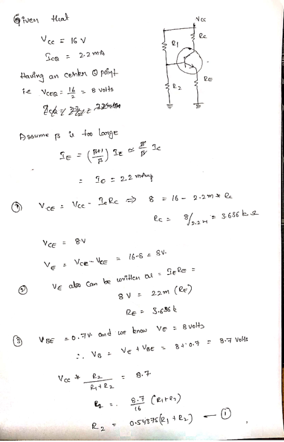
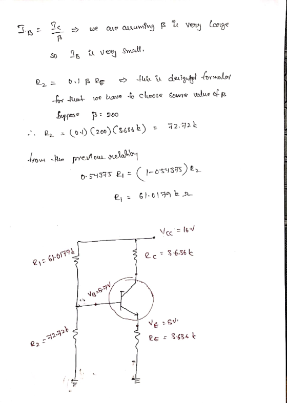
 [1] The circuit diagram on the left below is a common emitter amplifier. It is the full complement of components for this type of amplifier ready for AC analysis. This amplifier will be discussed in lecture prior to the lab exercises. However, with the circuit including only Rc. RE, Ri, and R2 as shown in the figure on the right, proceed with the design for a DC operating point of the common emitter amplifier. The following parameters are given: Vcc...
 5. Determine the Ico and Vceo for the emitter-biased common-emitter amplifier circuit show below. Assume B=180. (12 points) Vcc 918 v Rs12330 ks Rc 1,5 k22 Rs2 B V ce 18 220 ke2 RE 30.75 k2 6. Draw the circuit diagram of a common-emitter voltage-divider bias with the following parameters. (12 points) Vcc = 16V, R, -30k1, R2 = 10k22, Rc = 3.3kQ2, Re = 1.5k22, B = 199 (a) Determine lco and Vcro using the approximate method. (b) Determine...
 ASSUME ALL CAPACITORS ARE INFINITE
AND IDEAL.
For a common-emitter amplifier with a voltage divider bias configuration using a single source, and given Rs = 2009, Rc = R = 2k2, VBE = 0.7V, Vcc= 20V and B = 100: a. Find R. and R for maximum symmetric output swing b. Determine Vopp (ideal and practical) c. Sketch the dc and ac load lines, showing the q-point and all intercept values of voltage and current.
ASSUME ALL CAPACITORS ARE INFINITE
AND IDEAL.
For a common-emitter amplifier with a voltage divider bias configuration using a single source, and given Rs = 2009, Rc = R = 2k2, VBE = 0.7V, Vcc= 20V and B = 100: a. Find R. and R for maximum symmetric output swing b. Determine Vopp (ideal and practical) c. Sketch the dc and ac load lines, showing the q-point and all intercept values of voltage and current.
 Common-emitter amplifier?
(10 pts) Consider a common-emitter amplifier with emitter resistor shown below. DC voltage sources VBB and Vcc bias the transistor at lc-1mA. Let β-100. Determine the overall voltage gain Gv 2. VCC 10 k2 Vsig VBB
(10 pts) Consider a common-emitter amplifier with emitter resistor shown below. DC voltage sources VBB and Vcc bias the transistor at lc-1mA. Let β-100. Determine the overall voltage gain Gv 2. VCC 10 k2 Vsig VBB
Common-emitter amplifier?
(10 pts) Consider a common-emitter amplifier with emitter resistor shown below. DC voltage sources VBB and Vcc bias the transistor at lc-1mA. Let β-100. Determine the overall voltage gain Gv 2. VCC 10 k2 Vsig VBB
(10 pts) Consider a common-emitter amplifier with emitter resistor shown below. DC voltage sources VBB and Vcc bias the transistor at lc-1mA. Let β-100. Determine the overall voltage gain Gv 2. VCC 10 k2 Vsig VBB
 You are required to design a 2-stage voltage amplifier (find
values for RE, RC1, RC2) to meet the following criteria: an input
resistance of 400 kΩ and an overall voltage gain equal to or
greater than 250, with a resistor output load, RL. Use a
common-emitter with emitter degradation (RE) stage for the input,
followed by a commonemitter amplifier with bias current equal to
0.5 mA. (VCC = 20 V, βo = 200 and the DC levels of the first...
You are required to design a 2-stage voltage amplifier (find
values for RE, RC1, RC2) to meet the following criteria: an input
resistance of 400 kΩ and an overall voltage gain equal to or
greater than 250, with a resistor output load, RL. Use a
common-emitter with emitter degradation (RE) stage for the input,
followed by a commonemitter amplifier with bias current equal to
0.5 mA. (VCC = 20 V, βo = 200 and the DC levels of the first...
 (a) A voltage divider bypassed common-source (CS) FET amplifier biasing circuit with load R, is commonly used in electronic circuit. (1) Design the circuit of a voltage divider bypassed common-source FET amplifier biasing circuit with load Ru. [4 marks) (ii) By referring to Q4(a)(i), design a bypassed common-source FET amplifier with biasing voltage-divider to meet the given specifications below: Supply voltage, Vcc = 12 V; Voltage gain, Ay = -10; Output load Ru = 10 kV2; input impedance Zi =...
 4. For the emitter-resistor amplifier with a voltage divider bias configuration using a single source as shown to the right and given R-4892, R2 = 16k 2, RE = 20092, Rc = 1k2. RL = 2k12, Vec-20V, VBE = -0.7V, and B= 200. Find: a. lco and VCEO b. If beta varies between 150 and 250, is this circuit bias + stable? c. Fin ideal and practical values of the maximum symmetric output voltage swing.
 This direct coupled emitter follower amplifier using a reference current mirror to produce a blasttent for the di transistor The parameters for the circuit are as follows: . Vcc = -Ves = 5V • All transistors. Qı, Q2, Qs, are matched with the following parameters + 8 = 100 , Is = 10- A (Hints: You must solve for for all transistors. You may need to lerate once or twice to solve the recent with the foresistor in the Qiraulties...
 [1] The circuit diagram on the left below is a common emitter amplifier. It is the full complement of components for this type of amplifier ready for AC analysis. This amplifier will be discussed in lecture prior to the lab exercises. However, with the circuit including only Rc. RE, Ri, and R2 as shown in the figure on the right, proceed with the design for a DC operating point of the common emitter amplifier. The following parameters are given: Vcc...
Most questions answered within 3 hours.
-
The highly pathogenic bacterium Clostridium
perfringens causes gangrene, a disease that results in the
destruction of...
asked 11 minutes ago -
In the context of situation analysis, which of the following is
a category for analysis in...
asked 9 minutes ago -
In a study of the gas phase decomposition of sulfuryl chloride
at 600 K SO2Cl2(g)SO2(g) +...
asked 13 minutes ago -
75 g of 2-propanol (C3H8O) and 25 g of pentane are mixed in a
200 mL...
asked 14 minutes ago -
The 2800-turn coil in a dc motor has an area per turn of 1.1 ×
10-2...
asked 28 minutes ago -
Draw a combinational logic circuit diagram with a symbol inside
the box for two I/P of...
asked 30 minutes ago -
The cliché we use quite a lot in finance is: there is a need to
maximize...
asked 35 minutes ago -
In class we discussed the addition of HCl to alpha pinene. Would
you expect one or...
asked 36 minutes ago -
I'm trying to explain to my daughter to help her please help
me
I tagged the...
asked 43 minutes ago -
You want to accumulate $28,000 in 10 years using annual
payments, the first one in a...
asked 50 minutes ago -
1. Name the 4 products obtained from the reactions of the light phase of photosynthesis.
2....
asked 51 minutes ago -
An electron in an excited hydrogen atom makes two transitions.
First the electron drops from the...
asked 1 hour ago