
Homework Answers


Add Answer to:
This direct coupled emitter follower amplifier using a reference current mirror to produce a blasttent for...
Perform a simple initial design of an ac coupled common-emitter amplifier with four resistor biasing and emitter by-pass...
 Perform a simple initial design of an ac coupled common-emitter
amplifier with
four resistor biasing and emitter by-pass capacitor, to have a
voltage gain of about
100, for the following conditions. Justify any approximations used.
(Assume Ic=1/300 A)
i)Transistor ac common-emitter gain, B, 100 ii) Supply voltage ofV0c-20V iii) Allow 10% Vcc across RE DC collector voltage of 10 V iv) v) DC current in the base bias resistors should be ten times greater than the DC base current. Assume...
Perform a simple initial design of an ac coupled common-emitter
amplifier with
four resistor biasing and emitter by-pass capacitor, to have a
voltage gain of about
100, for the following conditions. Justify any approximations used.
(Assume Ic=1/300 A)
i)Transistor ac common-emitter gain, B, 100 ii) Supply voltage ofV0c-20V iii) Allow 10% Vcc across RE DC collector voltage of 10 V iv) v) DC current in the base bias resistors should be ten times greater than the DC base current. Assume...
Avec Úvo SRE L V II. (5pt) Consider the above-right common-collector or emitter-follower BJT amplifier circuit....
 Avec Úvo SRE L V II. (5pt) Consider the above-right common-collector or emitter-follower BJT amplifier circuit. Given: ß= 100, RE = 10 k1, Vcc = 20 V, RB = 5 k1, R1 = 10 kl, and Ry = 2 k1. (a) (1pt) Find the Q-point, i.e. Ibo, Ico, and VCEO; (b) (1pt) draw the small-signal equivalent circuit assuming that the capacitors (C, and Cy) are short circuits for the small signal; (c) (1pt) solve for the voltage gain, Av; (d)...
Student Assessment 1. The complementary PNP/NPN emitter follower circuit is intended as a: a small signal...
 Student Assessment 1. The complementary PNP/NPN emitter follower circuit is intended as a: a small signal voltage amplifier 6 high frequency amplifier. C high output impedance amplifier. d current/power amplifier 2. If a complementary PNP/NPN output pair is driven with dual polarity power () supplies then the input and output terminals will be at: a half of the positive supply voltage 6 0V (ground). C half of the negative supply voltage. a +0.6V. The Transfer Characteristic of a complementary PNP/NPN...
Solve for the following using: 1) exact method 2) approximate method compare if approximate method is...
 Solve for the following using:
1) exact method
2) approximate method
compare if approximate method is sufficient for analysis. which
solution is better?
Example For the voltage divider bias circuit, RB1-13K2, R 2.2k2 , Rc-68K(2. RE-1.5K(2.Vcc-15 V. VCEsat -0.3 V and β of the Si transistor is 80. Determine the following O" (a) DC base voltage and DC emitter voltage of the transistor amplifier (b) DC operating voltages and currents of the transistor amplifier (lBo, Ico, IEo and VcEO) (c)...
Solve for the following using:
1) exact method
2) approximate method
compare if approximate method is sufficient for analysis. which
solution is better?
Example For the voltage divider bias circuit, RB1-13K2, R 2.2k2 , Rc-68K(2. RE-1.5K(2.Vcc-15 V. VCEsat -0.3 V and β of the Si transistor is 80. Determine the following O" (a) DC base voltage and DC emitter voltage of the transistor amplifier (b) DC operating voltages and currents of the transistor amplifier (lBo, Ico, IEo and VcEO) (c)...
4. For the amplifier in the figure below use the parameters in the table: +Vcc Re VBE- 0.7V, Ri- ...
 4. For the amplifier in the figure below use the parameters in the table: +Vcc Re VBE- 0.7V, Ri- 1002, R1-160k2, R2-320k2 R3-200k2, R6-40 k2, Rc-60k2, Vcc- 12V, Ry Do a) Draw the DC equivalent circuit and calculate the Q-point. c) Draw the AC equivalent circuit with the small signal model for the transistor. d) Calculate the voltage gain, Av-Vo/vi. Assume ro infinite. e) Draw the circuit to find the amplifier input resistance (Rin). Calculate Rin f Draw the circuit...
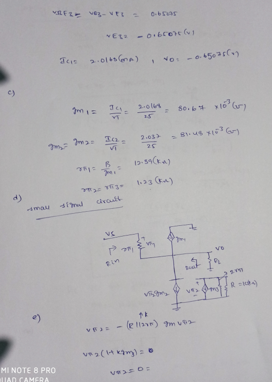
29. Identify the type of third stage amplifier: a) inverting amplifier; b) differential amplifier with passi load; c) differential amplifier with current mirror load; d) emitter follower; e...
 29. Identify the type of third stage amplifier: a) inverting amplifier; b) differential amplifier with passi load; c) differential amplifier with current mirror load; d) emitter follower; e) none of above; 30. The Vsg of Q5 should be: a)-1V, b)-0.85% c) 0.65% d)0.85% env 31. To obtain IREF-30μΑ , the value of R should be: a)250ohm; b)25Kohm; c)250Kohm; d)2.5Mohm; e 5Mohm. network is composed by 4 identical phase shifter. The phase shift of each phase shifter in degree should be...
8. Design the DC bias circuit of a voltage-divider biased common-emitter amplifier (12 points) with the...
 8. Design the DC bias circuit of a voltage-divider biased common-emitter amplifier (12 points) with the specification given below. Center Q-point, Vcc- 16V, Ico-2.2mA.
1. Two directly coupled common emitter amplifiers are shown below in Fig. 1. Since base current...
 1. Two directly coupled common emitter amplifiers are shown below in Fig. 1. Since base current IBase2 of the transistor Qp is much smaller than the collector current of QN, simply ignore I Base 2 current while solving the problem. Vsig is a purely AC signal. Find DC operating points (Ic, VCE) of the transistors. ON I Qp VA= OV B = 150 VE(ON) = 0.7 V VESAT) = 0.2 V VA= OV B = 70 V(ON) = 0.7 V...
Shown below is a single stage common emitter amplifier with a unipolar dc power supply using an 2...
 Shown below is a single stage common emitter amplifier with a unipolar dc power supply using an 2N3904 NPN BJT as the active device. It is specified that V+ 40 V, C1 C2CE 100uF, Ro-7.5 k2, REi-5.1kS2, and Ri - 36k52. Design the circuit so that the dc collector current is 2 mA and the magnitude of the small-signal midband voltage gain is 32.3. For the design calculations assume that the base-to- emitter dc voltage drop is 0.65 V, the...
can you do 4.83 Ar- Q Sea 100 V, what does the gain become? age at...
 can
you do 4.83
Ar- Q Sea 100 V, what does the gain become? age at the collector. (b) Replacing the transistor by its T model, da the small-signal equivalent circuit of the a plifier. Analyze the resulting circuit to dete mine the voltage gain t/ 04.81 Consider the CE amplifier circuit of Fig. 4.43(a). It is required to design the circuit (i.e., find values for I and Rc) to meet the following specifications: (a) R,5kn (b) the voltage gain...
can
you do 4.83
Ar- Q Sea 100 V, what does the gain become? age at the collector. (b) Replacing the transistor by its T model, da the small-signal equivalent circuit of the a plifier. Analyze the resulting circuit to dete mine the voltage gain t/ 04.81 Consider the CE amplifier circuit of Fig. 4.43(a). It is required to design the circuit (i.e., find values for I and Rc) to meet the following specifications: (a) R,5kn (b) the voltage gain...
 Perform a simple initial design of an ac coupled common-emitter
amplifier with
four resistor biasing and emitter by-pass capacitor, to have a
voltage gain of about
100, for the following conditions. Justify any approximations used.
(Assume Ic=1/300 A)
i)Transistor ac common-emitter gain, B, 100 ii) Supply voltage ofV0c-20V iii) Allow 10% Vcc across RE DC collector voltage of 10 V iv) v) DC current in the base bias resistors should be ten times greater than the DC base current. Assume...
Perform a simple initial design of an ac coupled common-emitter
amplifier with
four resistor biasing and emitter by-pass capacitor, to have a
voltage gain of about
100, for the following conditions. Justify any approximations used.
(Assume Ic=1/300 A)
i)Transistor ac common-emitter gain, B, 100 ii) Supply voltage ofV0c-20V iii) Allow 10% Vcc across RE DC collector voltage of 10 V iv) v) DC current in the base bias resistors should be ten times greater than the DC base current. Assume...
 Avec Úvo SRE L V II. (5pt) Consider the above-right common-collector or emitter-follower BJT amplifier circuit. Given: ß= 100, RE = 10 k1, Vcc = 20 V, RB = 5 k1, R1 = 10 kl, and Ry = 2 k1. (a) (1pt) Find the Q-point, i.e. Ibo, Ico, and VCEO; (b) (1pt) draw the small-signal equivalent circuit assuming that the capacitors (C, and Cy) are short circuits for the small signal; (c) (1pt) solve for the voltage gain, Av; (d)...
 Student Assessment 1. The complementary PNP/NPN emitter follower circuit is intended as a: a small signal voltage amplifier 6 high frequency amplifier. C high output impedance amplifier. d current/power amplifier 2. If a complementary PNP/NPN output pair is driven with dual polarity power () supplies then the input and output terminals will be at: a half of the positive supply voltage 6 0V (ground). C half of the negative supply voltage. a +0.6V. The Transfer Characteristic of a complementary PNP/NPN...
 Solve for the following using:
1) exact method
2) approximate method
compare if approximate method is sufficient for analysis. which
solution is better?
Example For the voltage divider bias circuit, RB1-13K2, R 2.2k2 , Rc-68K(2. RE-1.5K(2.Vcc-15 V. VCEsat -0.3 V and β of the Si transistor is 80. Determine the following O" (a) DC base voltage and DC emitter voltage of the transistor amplifier (b) DC operating voltages and currents of the transistor amplifier (lBo, Ico, IEo and VcEO) (c)...
Solve for the following using:
1) exact method
2) approximate method
compare if approximate method is sufficient for analysis. which
solution is better?
Example For the voltage divider bias circuit, RB1-13K2, R 2.2k2 , Rc-68K(2. RE-1.5K(2.Vcc-15 V. VCEsat -0.3 V and β of the Si transistor is 80. Determine the following O" (a) DC base voltage and DC emitter voltage of the transistor amplifier (b) DC operating voltages and currents of the transistor amplifier (lBo, Ico, IEo and VcEO) (c)...
 4. For the amplifier in the figure below use the parameters in the table: +Vcc Re VBE- 0.7V, Ri- 1002, R1-160k2, R2-320k2 R3-200k2, R6-40 k2, Rc-60k2, Vcc- 12V, Ry Do a) Draw the DC equivalent circuit and calculate the Q-point. c) Draw the AC equivalent circuit with the small signal model for the transistor. d) Calculate the voltage gain, Av-Vo/vi. Assume ro infinite. e) Draw the circuit to find the amplifier input resistance (Rin). Calculate Rin f Draw the circuit...
 29. Identify the type of third stage amplifier: a) inverting amplifier; b) differential amplifier with passi load; c) differential amplifier with current mirror load; d) emitter follower; e) none of above; 30. The Vsg of Q5 should be: a)-1V, b)-0.85% c) 0.65% d)0.85% env 31. To obtain IREF-30μΑ , the value of R should be: a)250ohm; b)25Kohm; c)250Kohm; d)2.5Mohm; e 5Mohm. network is composed by 4 identical phase shifter. The phase shift of each phase shifter in degree should be...
 8. Design the DC bias circuit of a voltage-divider biased common-emitter amplifier (12 points) with the specification given below. Center Q-point, Vcc- 16V, Ico-2.2mA.
 1. Two directly coupled common emitter amplifiers are shown below in Fig. 1. Since base current IBase2 of the transistor Qp is much smaller than the collector current of QN, simply ignore I Base 2 current while solving the problem. Vsig is a purely AC signal. Find DC operating points (Ic, VCE) of the transistors. ON I Qp VA= OV B = 150 VE(ON) = 0.7 V VESAT) = 0.2 V VA= OV B = 70 V(ON) = 0.7 V...
 Shown below is a single stage common emitter amplifier with a unipolar dc power supply using an 2N3904 NPN BJT as the active device. It is specified that V+ 40 V, C1 C2CE 100uF, Ro-7.5 k2, REi-5.1kS2, and Ri - 36k52. Design the circuit so that the dc collector current is 2 mA and the magnitude of the small-signal midband voltage gain is 32.3. For the design calculations assume that the base-to- emitter dc voltage drop is 0.65 V, the...
 can
you do 4.83
Ar- Q Sea 100 V, what does the gain become? age at the collector. (b) Replacing the transistor by its T model, da the small-signal equivalent circuit of the a plifier. Analyze the resulting circuit to dete mine the voltage gain t/ 04.81 Consider the CE amplifier circuit of Fig. 4.43(a). It is required to design the circuit (i.e., find values for I and Rc) to meet the following specifications: (a) R,5kn (b) the voltage gain...
can
you do 4.83
Ar- Q Sea 100 V, what does the gain become? age at the collector. (b) Replacing the transistor by its T model, da the small-signal equivalent circuit of the a plifier. Analyze the resulting circuit to dete mine the voltage gain t/ 04.81 Consider the CE amplifier circuit of Fig. 4.43(a). It is required to design the circuit (i.e., find values for I and Rc) to meet the following specifications: (a) R,5kn (b) the voltage gain...
Most questions answered within 3 hours.
-
You have a 825.3 mL sample of 2.754 M HA (Ka =
4.49⋅10−4). Calculate the pH...
asked 14 minutes ago -
The blues made its way into many kinds of music. Eric Clapton,
The Beatles, and Elvis...
asked 2 hours ago -
8. A wave in a string has a wave function given by: y (x, t) =...
asked 1 hour ago -
If you’re standing at the bottom of a hill and asked to evaluate
it while being...
asked 3 hours ago -
1. Which region has taken the lead in the world of
e-waste handling?
a) European Union...
asked 3 hours ago -
A 8.15- g bullet from a 9-mm pistol has a velocity of 366.0 m/s.
It strikes...
asked 4 hours ago -
The outstanding bonds of Alpha Extracts have a yield to maturity
of 7.4 percent and a...
asked 4 hours ago -
The Problem: The Case of the Harmonizing Vacations
Your CEO is exploring partnering with a European...
asked 5 hours ago -
A chemical equation is balanced by adding coefficients in front
of some formulas so that the...
asked 5 hours ago -
From the literature (reference your sources): What are the
lattice parameters of calcite and aragonite? Why...
asked 6 hours ago -
Your system is rejecting the question am asking which is
preceded by a case study. It...
asked 6 hours ago -
3. On January 2, 2000, Larry creates a trust with himself as
trustee. Larry as trustee...
asked 6 hours ago