
Homework Answers
Add Answer to:
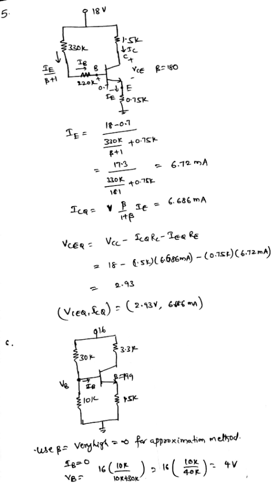
5. Determine the Ico and Vceo for the emitter-biased common-emitter amplifier circuit show below. Assume B=180....
8. Design the DC bias circuit of a voltage-divider biased common-emitter amplifier (12 points) with the...
 8. Design the DC bias circuit of a voltage-divider biased common-emitter amplifier (12 points) with the specification given below. Center Q-point, Vcc- 16V, Ico-2.2mA.
[1] The circuit diagram on the left below is a common emitter amplifier. It is the...
 [1] The circuit diagram on the left below is a common emitter amplifier. It is the full complement of components for this type of amplifier ready for AC analysis. This amplifier will be discussed in lecture prior to the lab exercises. However, with the circuit including only Rc. RE, Ri, and R2 as shown in the figure on the right, proceed with the design for a DC operating point of the common emitter amplifier. The following parameters are given: Vcc...
4. For the emitter-resistor amplifier with a voltage divider bias configuration using a single source as...
 4. For the emitter-resistor amplifier with a voltage divider bias configuration using a single source as shown to the right and given R-4892, R2 = 16k 2, RE = 20092, Rc = 1k2. RL = 2k12, Vec-20V, VBE = -0.7V, and B= 200. Find: a. lco and VCEO b. If beta varies between 150 and 250, is this circuit bias + stable? c. Fin ideal and practical values of the maximum symmetric output voltage swing.
Solve for the following using: 1) exact method 2) approximate method compare if approximate method is...
 Solve for the following using:
1) exact method
2) approximate method
compare if approximate method is sufficient for analysis. which
solution is better?
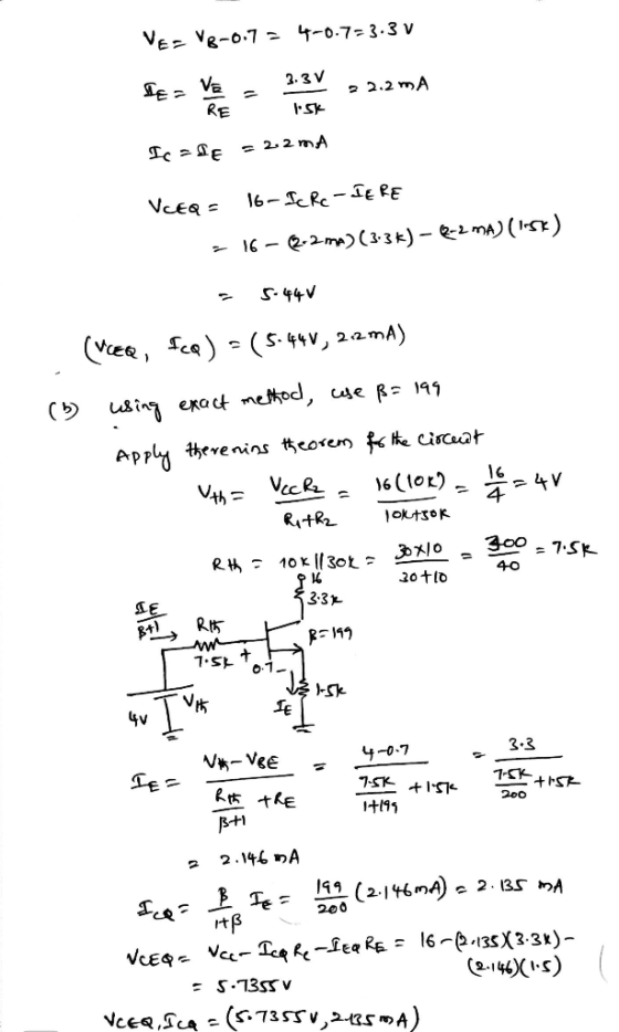
Example For the voltage divider bias circuit, RB1-13K2, R 2.2k2 , Rc-68K(2. RE-1.5K(2.Vcc-15 V. VCEsat -0.3 V and β of the Si transistor is 80. Determine the following O" (a) DC base voltage and DC emitter voltage of the transistor amplifier (b) DC operating voltages and currents of the transistor amplifier (lBo, Ico, IEo and VcEO) (c)...
Solve for the following using:
1) exact method
2) approximate method
compare if approximate method is sufficient for analysis. which
solution is better?
Example For the voltage divider bias circuit, RB1-13K2, R 2.2k2 , Rc-68K(2. RE-1.5K(2.Vcc-15 V. VCEsat -0.3 V and β of the Si transistor is 80. Determine the following O" (a) DC base voltage and DC emitter voltage of the transistor amplifier (b) DC operating voltages and currents of the transistor amplifier (lBo, Ico, IEo and VcEO) (c)...
Avec Úvo SRE L V II. (5pt) Consider the above-right common-collector or emitter-follower BJT amplifier circuit....
 Avec Úvo SRE L V II. (5pt) Consider the above-right common-collector or emitter-follower BJT amplifier circuit. Given: ß= 100, RE = 10 k1, Vcc = 20 V, RB = 5 k1, R1 = 10 kl, and Ry = 2 k1. (a) (1pt) Find the Q-point, i.e. Ibo, Ico, and VCEO; (b) (1pt) draw the small-signal equivalent circuit assuming that the capacitors (C, and Cy) are short circuits for the small signal; (c) (1pt) solve for the voltage gain, Av; (d)...
1. Consider the Common-Emitter BJT amplifier circuit, shown below. VD VOD BJT Parameters: B=99 A/A i=0...
 1. Consider the Common-Emitter BJT amplifier circuit, shown below. VD VOD BJT Parameters: B=99 A/A i=0 RE Co Circuit Parameters: Ca Cc2 = 0 F Car = OF R = 2022 R = 2002 R1 = 25.8 k22 Ry2 = 51.6 ks V = 15 V VEE=0 V Сct Active Mode: Va >0.2 V Vwx=0.7V Ic=B1, Ic=al, 1 R2 3 SRCA a) Find the open-circuit voltage gain, Ave, of this amplifier circuit. Verify your assumptions. b) Compute the input resistance,...
Calculate the voltage gain (Av) for the loaded Common Emitter Amplifier below: BAC 200 for all...
 Calculate the voltage gain (Av) for the loaded Common Emitter Amplifier below: BAC 200 for all transistors. Assume re 15 Q for the CE Amplifier. Ignore re' for the DP Amplifier Vcc 12 V, R1 56 K, R2 10 KQ, R4 22 KQ R3 5.6 KQ, RL 8 RE(CE) 628 0, RE(CC) 330 Rc 3.5 KQ, Enter your results. No units. SR3 R1 RC C3 Vcc C1 Beta Q2a HH Vin Beta Q1 Beta Q2b C4 R4 Vs R2 C2...
2. For the common-emitter amplifier. B= 50. Vcc=12 a) Draw small signal circuit b) Find vout/vin...
 2. For the common-emitter amplifier. B= 50. Vcc=12 a) Draw small signal circuit b) Find vout/vin Find Zin and Zou Vcc R1 27k R2 2.2k Zout Zin Vo 4 C1 16 BIG Q1 NPN V1 C2 V R3 15k RE 1.2k BIG
ASSUME ALL CAPACITORS ARE INFINITE AND IDEAL. For a common-emitter amplifier with a voltage divider bias...
 ASSUME ALL CAPACITORS ARE INFINITE
AND IDEAL.
For a common-emitter amplifier with a voltage divider bias configuration using a single source, and given Rs = 2009, Rc = R = 2k2, VBE = 0.7V, Vcc= 20V and B = 100: a. Find R. and R for maximum symmetric output swing b. Determine Vopp (ideal and practical) c. Sketch the dc and ac load lines, showing the q-point and all intercept values of voltage and current.
ASSUME ALL CAPACITORS ARE INFINITE
AND IDEAL.
For a common-emitter amplifier with a voltage divider bias configuration using a single source, and given Rs = 2009, Rc = R = 2k2, VBE = 0.7V, Vcc= 20V and B = 100: a. Find R. and R for maximum symmetric output swing b. Determine Vopp (ideal and practical) c. Sketch the dc and ac load lines, showing the q-point and all intercept values of voltage and current.
FIND THE VALUES OF Rb1, Rb2, Re,Rc, rin , rout, overall gain and open circuit gain First, design a common emitter BJT a...
 FIND THE VALUES OF Rb1, Rb2, Re,Rc, rin , rout, overall gain and
open circuit gain
First, design a common emitter BJT amplifier Second, analyze the amplifier.( Avo, Gv, Rin, Rout) Third, compare your calculation with Multisim. Report must include comparison between your calculation & simulation results overall voltage gain, open circuit voltage gain, input resistance, and output resistance. This design project is not group work, must be done individually. Type your report. Design a discrete common emitter BJT amplifier.(Determine...
FIND THE VALUES OF Rb1, Rb2, Re,Rc, rin , rout, overall gain and
open circuit gain
First, design a common emitter BJT amplifier Second, analyze the amplifier.( Avo, Gv, Rin, Rout) Third, compare your calculation with Multisim. Report must include comparison between your calculation & simulation results overall voltage gain, open circuit voltage gain, input resistance, and output resistance. This design project is not group work, must be done individually. Type your report. Design a discrete common emitter BJT amplifier.(Determine...
 8. Design the DC bias circuit of a voltage-divider biased common-emitter amplifier (12 points) with the specification given below. Center Q-point, Vcc- 16V, Ico-2.2mA.
 [1] The circuit diagram on the left below is a common emitter amplifier. It is the full complement of components for this type of amplifier ready for AC analysis. This amplifier will be discussed in lecture prior to the lab exercises. However, with the circuit including only Rc. RE, Ri, and R2 as shown in the figure on the right, proceed with the design for a DC operating point of the common emitter amplifier. The following parameters are given: Vcc...
 4. For the emitter-resistor amplifier with a voltage divider bias configuration using a single source as shown to the right and given R-4892, R2 = 16k 2, RE = 20092, Rc = 1k2. RL = 2k12, Vec-20V, VBE = -0.7V, and B= 200. Find: a. lco and VCEO b. If beta varies between 150 and 250, is this circuit bias + stable? c. Fin ideal and practical values of the maximum symmetric output voltage swing.
 Solve for the following using:
1) exact method
2) approximate method
compare if approximate method is sufficient for analysis. which
solution is better?
Example For the voltage divider bias circuit, RB1-13K2, R 2.2k2 , Rc-68K(2. RE-1.5K(2.Vcc-15 V. VCEsat -0.3 V and β of the Si transistor is 80. Determine the following O" (a) DC base voltage and DC emitter voltage of the transistor amplifier (b) DC operating voltages and currents of the transistor amplifier (lBo, Ico, IEo and VcEO) (c)...
Solve for the following using:
1) exact method
2) approximate method
compare if approximate method is sufficient for analysis. which
solution is better?
Example For the voltage divider bias circuit, RB1-13K2, R 2.2k2 , Rc-68K(2. RE-1.5K(2.Vcc-15 V. VCEsat -0.3 V and β of the Si transistor is 80. Determine the following O" (a) DC base voltage and DC emitter voltage of the transistor amplifier (b) DC operating voltages and currents of the transistor amplifier (lBo, Ico, IEo and VcEO) (c)...
 Avec Úvo SRE L V II. (5pt) Consider the above-right common-collector or emitter-follower BJT amplifier circuit. Given: ß= 100, RE = 10 k1, Vcc = 20 V, RB = 5 k1, R1 = 10 kl, and Ry = 2 k1. (a) (1pt) Find the Q-point, i.e. Ibo, Ico, and VCEO; (b) (1pt) draw the small-signal equivalent circuit assuming that the capacitors (C, and Cy) are short circuits for the small signal; (c) (1pt) solve for the voltage gain, Av; (d)...
 1. Consider the Common-Emitter BJT amplifier circuit, shown below. VD VOD BJT Parameters: B=99 A/A i=0 RE Co Circuit Parameters: Ca Cc2 = 0 F Car = OF R = 2022 R = 2002 R1 = 25.8 k22 Ry2 = 51.6 ks V = 15 V VEE=0 V Сct Active Mode: Va >0.2 V Vwx=0.7V Ic=B1, Ic=al, 1 R2 3 SRCA a) Find the open-circuit voltage gain, Ave, of this amplifier circuit. Verify your assumptions. b) Compute the input resistance,...
 Calculate the voltage gain (Av) for the loaded Common Emitter Amplifier below: BAC 200 for all transistors. Assume re 15 Q for the CE Amplifier. Ignore re' for the DP Amplifier Vcc 12 V, R1 56 K, R2 10 KQ, R4 22 KQ R3 5.6 KQ, RL 8 RE(CE) 628 0, RE(CC) 330 Rc 3.5 KQ, Enter your results. No units. SR3 R1 RC C3 Vcc C1 Beta Q2a HH Vin Beta Q1 Beta Q2b C4 R4 Vs R2 C2...
 2. For the common-emitter amplifier. B= 50. Vcc=12 a) Draw small signal circuit b) Find vout/vin Find Zin and Zou Vcc R1 27k R2 2.2k Zout Zin Vo 4 C1 16 BIG Q1 NPN V1 C2 V R3 15k RE 1.2k BIG
 ASSUME ALL CAPACITORS ARE INFINITE
AND IDEAL.
For a common-emitter amplifier with a voltage divider bias configuration using a single source, and given Rs = 2009, Rc = R = 2k2, VBE = 0.7V, Vcc= 20V and B = 100: a. Find R. and R for maximum symmetric output swing b. Determine Vopp (ideal and practical) c. Sketch the dc and ac load lines, showing the q-point and all intercept values of voltage and current.
ASSUME ALL CAPACITORS ARE INFINITE
AND IDEAL.
For a common-emitter amplifier with a voltage divider bias configuration using a single source, and given Rs = 2009, Rc = R = 2k2, VBE = 0.7V, Vcc= 20V and B = 100: a. Find R. and R for maximum symmetric output swing b. Determine Vopp (ideal and practical) c. Sketch the dc and ac load lines, showing the q-point and all intercept values of voltage and current.
 FIND THE VALUES OF Rb1, Rb2, Re,Rc, rin , rout, overall gain and
open circuit gain
First, design a common emitter BJT amplifier Second, analyze the amplifier.( Avo, Gv, Rin, Rout) Third, compare your calculation with Multisim. Report must include comparison between your calculation & simulation results overall voltage gain, open circuit voltage gain, input resistance, and output resistance. This design project is not group work, must be done individually. Type your report. Design a discrete common emitter BJT amplifier.(Determine...
FIND THE VALUES OF Rb1, Rb2, Re,Rc, rin , rout, overall gain and
open circuit gain
First, design a common emitter BJT amplifier Second, analyze the amplifier.( Avo, Gv, Rin, Rout) Third, compare your calculation with Multisim. Report must include comparison between your calculation & simulation results overall voltage gain, open circuit voltage gain, input resistance, and output resistance. This design project is not group work, must be done individually. Type your report. Design a discrete common emitter BJT amplifier.(Determine...
Most questions answered within 3 hours.
-
Ken believes the average age of men who come to get a haircut at
his barber...
asked 6 minutes ago -
(Ratio Analysis): Last year Co. XYZ had sales of $ 400,000, with
“cost of goods sold”...
asked 14 minutes ago -
can someone please write the balanced chemical
equation for the synthesis of Bromoacetanilide
from;
aniline +...
asked 10 minutes ago -
1. If a corporation purchases land and building and subsequently
tears down the building and uses...
asked 21 minutes ago -
Consider a 23-year bond with 7 percent annual coupon payments.
The market rate (YTM) is 6.4...
asked 24 minutes ago -
a tuba creates a 4th harmonic of frequency 116.5 Hz. what is the
frequency of the...
asked 31 minutes ago -
A coconut mass 2kg falls from a 30m tall tree. The coconut falls
and comes to...
asked 34 minutes ago -
Group Policies
Research GROUP POLICY OBJECTS (GPO'S)
You can start in the Windows Server 2012 eBook...
asked 38 minutes ago -
software engineering
Problems.
Create a use case diagram for class registration for a
university.
Create a...
asked 37 minutes ago -
You are trying to convince your friend who wants to attend
medical school to take BY123...
asked 53 minutes ago -
Subject: C++
I have created a class called QueueOfIntegers in a file called
QueueOfIntegers.h, which is...
asked 52 minutes ago -
calculate the number of molecules of gas in a
container of 2.0 liter at 30 degrees...
asked 1 hour ago