
Homework Answers
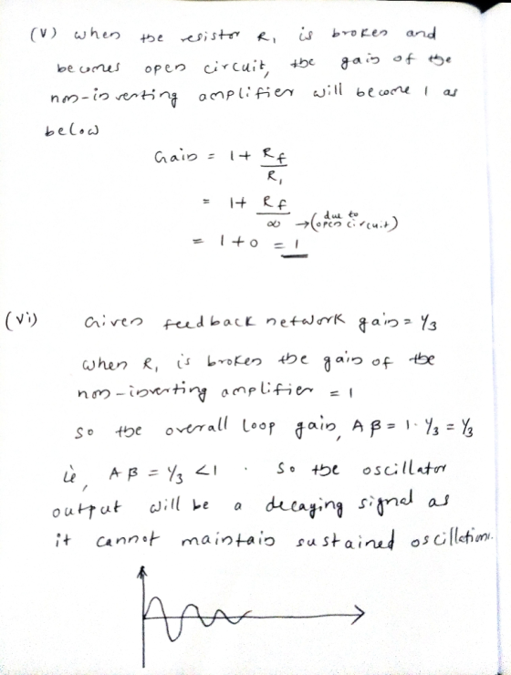
(i) Feedback network contains bridge network which does not provide phase shift at oscillating frequency as one arm consists of lead circuit and other arm consists of lag circuit. The total phase shift around the loop is zero as the bridge network and the noninverting amplifier does not give any phase shift. So the components R2,C2,R3, and C3 contribute to the positive feedback network.
Add Answer to:
need to help do this question,thanks
(c) Figure 3 shows the schematic diagram of a typical...
EEET255 Electronics Page 4 of6 QUESTION 3: [25 marks] Figure 3 shows a feedback amplifier circuit...
 EEET255 Electronics Page 4 of6 QUESTION 3: [25 marks] Figure 3 shows a feedback amplifier circuit R, is the source resistor, R is the feedback resistor and R, is the load resistor. The op-amp has an internal input resistance of R, an intemal output resistance R, and an internal gain of A Apply the "Systematic Analysis" method in this question. Figure 3 3.a State the feedback topology used in the amplifier circuit and which type of feedback amplifier is shown...
need help with C and D please The differentiator circuit shown in Figure 1 uses an op-amp with ideal characteristics. R2 R1 C1 Vi O Figure 1 (c) Sketch the Bode magnitude response for this circ...
 need help with C and D please
The differentiator circuit shown in Figure 1 uses an op-amp with ideal characteristics. R2 R1 C1 Vi O Figure 1 (c) Sketch the Bode magnitude response for this circuit for the frequency range of 10° to 108 Hz. (7 marks) (d) Sketch the output waveform of the differentiator and justify your answer, if v is as shown in Figure 2 with a period of: () 100 ms (ii) 10 us (6 marks) 0.11...
need help with C and D please
The differentiator circuit shown in Figure 1 uses an op-amp with ideal characteristics. R2 R1 C1 Vi O Figure 1 (c) Sketch the Bode magnitude response for this circuit for the frequency range of 10° to 108 Hz. (7 marks) (d) Sketch the output waveform of the differentiator and justify your answer, if v is as shown in Figure 2 with a period of: () 100 ms (ii) 10 us (6 marks) 0.11...
Circuit Analysis Vcc +Vcc 10 k2 R3 1kn 4 1 k2 Voi 7 555 A oVo...
 Circuit Analysis
Vcc +Vcc 10 k2 R3 1kn 4 1 k2 Voi 7 555 A oVo 3 555 2 R4 10 kn R2 2 1 MQ 5 5 6 C1 1 F C3 0.1 uF C4 10 nF C2 10 nF I Figure Q2 4 Figure Q2 shows an oscillator circuit using two 555 timers. Assume that the reset pin is active low. When the switch is opened: (i) Draw the output waveform (V01) of Timer A indicating clearly the...
Circuit Analysis
Vcc +Vcc 10 k2 R3 1kn 4 1 k2 Voi 7 555 A oVo 3 555 2 R4 10 kn R2 2 1 MQ 5 5 6 C1 1 F C3 0.1 uF C4 10 nF C2 10 nF I Figure Q2 4 Figure Q2 shows an oscillator circuit using two 555 timers. Assume that the reset pin is active low. When the switch is opened: (i) Draw the output waveform (V01) of Timer A indicating clearly the...
Figure 2 shows a multiple op-amp networks combined to produce a gain amplifier circuit. For the...
 Figure 2 shows a multiple op-amp networks combined to produce a gain amplifier circuit. For the given circuit: (i) Name all the type of op-amp circuits shown by Op-Amp 1 until Op-Amp 5. (ii) Calculate the output of each Op-Amp 1 until Op-Amp 4. Assume Vin = 10mV (iii) Determine the output voltage at the last Op-Amp 5. From this value, calculate the gain produced by this Op-Amp network in overall, by using Av=Vos / Vin equation. [10 Marks] CO3,...
ONLY NEED HELP WITH C AND D PLEASE! The differentiator circuit shown in Figure 1 uses an op-amp with ideal characteristics C1 Figure 1 (a) Prove that the gain of the circuit is given by the following...
 ONLY NEED HELP WITH C AND D PLEASE!
The differentiator circuit shown in Figure 1 uses an op-amp with ideal characteristics C1 Figure 1 (a) Prove that the gain of the circuit is given by the following expression using first principles for an ideal op-amp (2 marks) Gain = - (1 + juli R 1) (b) If the differentiator frequency (at unity gain) is 100Hz and the high frequency gain is 40dB and R2 is 220kQ, design the rest of...
ONLY NEED HELP WITH C AND D PLEASE!
The differentiator circuit shown in Figure 1 uses an op-amp with ideal characteristics C1 Figure 1 (a) Prove that the gain of the circuit is given by the following expression using first principles for an ideal op-amp (2 marks) Gain = - (1 + juli R 1) (b) If the differentiator frequency (at unity gain) is 100Hz and the high frequency gain is 40dB and R2 is 220kQ, design the rest of...
(a) Design a inverting Schmitt trigger circuit to be used as a zero crossing detector with transition voltages about ±25...
 (a) Design a inverting Schmitt trigger circuit
to be used as a zero crossing detector with transition voltages
about ±25 mV. Assume the saturation voltages for the op–amp are ±13
V. Draw the voltage transfer characteristic (VTC), i.e., vout vs.
vin.
(b) Design an astable multivibrator to produce
a square signal with a frequency of 1 kHz using C=0.01 µF, R1 = 30
kΩ, and R2 = 20 kΩ. Sketch the circuit waveforms (vo, v +, and v −)
assuming...
(a) Design a inverting Schmitt trigger circuit
to be used as a zero crossing detector with transition voltages
about ±25 mV. Assume the saturation voltages for the op–amp are ±13
V. Draw the voltage transfer characteristic (VTC), i.e., vout vs.
vin.
(b) Design an astable multivibrator to produce
a square signal with a frequency of 1 kHz using C=0.01 µF, R1 = 30
kΩ, and R2 = 20 kΩ. Sketch the circuit waveforms (vo, v +, and v −)
assuming...
a The operational amplifier in Figure 3.a has a slew rate of 0.5V/us and a unity gain bandwid of 5 MHz. Determine () the voltage gain, and (ii) the maximum input frequency such that the output wa...
 a The operational amplifier in Figure 3.a has a slew rate of 0.5V/us and a unity gain bandwid of 5 MHz. Determine () the voltage gain, and (ii) the maximum input frequency such that the output waveform is undistorted. with Vpeak 1V and frequency f. () Determine the cutoff frequency, (ii) plot, to scale, the you use this integrator if the input frequency is 30 KHz? Explain your answer. that any feedback resistance is fixed to 5k2. b. In the...
ONLY NEED HELP WITH III and IV PLEASE (e) A second stage, shown in Figure 3, is cascaded directly after the output of the circuit in Figure 1 R4 Figure 3 (i) Show that the combined response of the c...
 ONLY NEED HELP WITH III and IV PLEASE
(e) A second stage, shown in Figure 3, is cascaded directly after the output of the circuit in Figure 1 R4 Figure 3 (i) Show that the combined response of the complete circuit is given by: (4 marks) (ii) The two cascaded stages form a bandpass filter, which only amplifies a specific range of frequencies. This range of frequencies is known as the passband. Using the values chosen in (a) for Figure...
ONLY NEED HELP WITH III and IV PLEASE
(e) A second stage, shown in Figure 3, is cascaded directly after the output of the circuit in Figure 1 R4 Figure 3 (i) Show that the combined response of the complete circuit is given by: (4 marks) (ii) The two cascaded stages form a bandpass filter, which only amplifies a specific range of frequencies. This range of frequencies is known as the passband. Using the values chosen in (a) for Figure...
Problem 2 Consider the feedback amplifier circuit on Figure P2. The DC current gain of transistor Q3 is -100 1. What type of feedback (or what feedback topology) do we have on the circuit in Figure P...
 Problem 2 Consider the feedback amplifier circuit on Figure P2. The DC current gain of transistor Q3 is -100 1. What type of feedback (or what feedback topology) do we have on the circuit in Figure P2? 2. Draw the A-circuit. Express and compute the open-loop voltage gain A at mid-band frequency 3, Draw the γ-circuit. Express and compute the feedback factor γ 4. Express and compute the overall gain of the feedback amplifier Ap Express and compute the input...
Question 10 (5 marks) A combinational logic circuit is shown in Figure 3 along with a timing diagram. a) The output waveform (X) shown in the timing diagram is not correct for the circuit shown....
 Question 10 (5 marks) A combinational logic circuit is shown in Figure 3 along with a timing diagram. a) The output waveform (X) shown in the timing diagram is not correct for the circuit shown. Draw the correct waveform. (2 marks) b) The output waveform shown is the result of incorrect implementation of the circuit gates has been replaced by another type of gate. Which gate has been replaced and what is the replacement gate? Explain your answer. (3 marks)...
 EEET255 Electronics Page 4 of6 QUESTION 3: [25 marks] Figure 3 shows a feedback amplifier circuit R, is the source resistor, R is the feedback resistor and R, is the load resistor. The op-amp has an internal input resistance of R, an intemal output resistance R, and an internal gain of A Apply the "Systematic Analysis" method in this question. Figure 3 3.a State the feedback topology used in the amplifier circuit and which type of feedback amplifier is shown...
 need help with C and D please
The differentiator circuit shown in Figure 1 uses an op-amp with ideal characteristics. R2 R1 C1 Vi O Figure 1 (c) Sketch the Bode magnitude response for this circuit for the frequency range of 10° to 108 Hz. (7 marks) (d) Sketch the output waveform of the differentiator and justify your answer, if v is as shown in Figure 2 with a period of: () 100 ms (ii) 10 us (6 marks) 0.11...
need help with C and D please
The differentiator circuit shown in Figure 1 uses an op-amp with ideal characteristics. R2 R1 C1 Vi O Figure 1 (c) Sketch the Bode magnitude response for this circuit for the frequency range of 10° to 108 Hz. (7 marks) (d) Sketch the output waveform of the differentiator and justify your answer, if v is as shown in Figure 2 with a period of: () 100 ms (ii) 10 us (6 marks) 0.11...
 Circuit Analysis
Vcc +Vcc 10 k2 R3 1kn 4 1 k2 Voi 7 555 A oVo 3 555 2 R4 10 kn R2 2 1 MQ 5 5 6 C1 1 F C3 0.1 uF C4 10 nF C2 10 nF I Figure Q2 4 Figure Q2 shows an oscillator circuit using two 555 timers. Assume that the reset pin is active low. When the switch is opened: (i) Draw the output waveform (V01) of Timer A indicating clearly the...
Circuit Analysis
Vcc +Vcc 10 k2 R3 1kn 4 1 k2 Voi 7 555 A oVo 3 555 2 R4 10 kn R2 2 1 MQ 5 5 6 C1 1 F C3 0.1 uF C4 10 nF C2 10 nF I Figure Q2 4 Figure Q2 shows an oscillator circuit using two 555 timers. Assume that the reset pin is active low. When the switch is opened: (i) Draw the output waveform (V01) of Timer A indicating clearly the...
 Figure 2 shows a multiple op-amp networks combined to produce a gain amplifier circuit. For the given circuit: (i) Name all the type of op-amp circuits shown by Op-Amp 1 until Op-Amp 5. (ii) Calculate the output of each Op-Amp 1 until Op-Amp 4. Assume Vin = 10mV (iii) Determine the output voltage at the last Op-Amp 5. From this value, calculate the gain produced by this Op-Amp network in overall, by using Av=Vos / Vin equation. [10 Marks] CO3,...
 ONLY NEED HELP WITH C AND D PLEASE!
The differentiator circuit shown in Figure 1 uses an op-amp with ideal characteristics C1 Figure 1 (a) Prove that the gain of the circuit is given by the following expression using first principles for an ideal op-amp (2 marks) Gain = - (1 + juli R 1) (b) If the differentiator frequency (at unity gain) is 100Hz and the high frequency gain is 40dB and R2 is 220kQ, design the rest of...
ONLY NEED HELP WITH C AND D PLEASE!
The differentiator circuit shown in Figure 1 uses an op-amp with ideal characteristics C1 Figure 1 (a) Prove that the gain of the circuit is given by the following expression using first principles for an ideal op-amp (2 marks) Gain = - (1 + juli R 1) (b) If the differentiator frequency (at unity gain) is 100Hz and the high frequency gain is 40dB and R2 is 220kQ, design the rest of...
 (a) Design a inverting Schmitt trigger circuit
to be used as a zero crossing detector with transition voltages
about ±25 mV. Assume the saturation voltages for the op–amp are ±13
V. Draw the voltage transfer characteristic (VTC), i.e., vout vs.
vin.
(b) Design an astable multivibrator to produce
a square signal with a frequency of 1 kHz using C=0.01 µF, R1 = 30
kΩ, and R2 = 20 kΩ. Sketch the circuit waveforms (vo, v +, and v −)
assuming...
(a) Design a inverting Schmitt trigger circuit
to be used as a zero crossing detector with transition voltages
about ±25 mV. Assume the saturation voltages for the op–amp are ±13
V. Draw the voltage transfer characteristic (VTC), i.e., vout vs.
vin.
(b) Design an astable multivibrator to produce
a square signal with a frequency of 1 kHz using C=0.01 µF, R1 = 30
kΩ, and R2 = 20 kΩ. Sketch the circuit waveforms (vo, v +, and v −)
assuming...
 a The operational amplifier in Figure 3.a has a slew rate of 0.5V/us and a unity gain bandwid of 5 MHz. Determine () the voltage gain, and (ii) the maximum input frequency such that the output waveform is undistorted. with Vpeak 1V and frequency f. () Determine the cutoff frequency, (ii) plot, to scale, the you use this integrator if the input frequency is 30 KHz? Explain your answer. that any feedback resistance is fixed to 5k2. b. In the...
 ONLY NEED HELP WITH III and IV PLEASE
(e) A second stage, shown in Figure 3, is cascaded directly after the output of the circuit in Figure 1 R4 Figure 3 (i) Show that the combined response of the complete circuit is given by: (4 marks) (ii) The two cascaded stages form a bandpass filter, which only amplifies a specific range of frequencies. This range of frequencies is known as the passband. Using the values chosen in (a) for Figure...
ONLY NEED HELP WITH III and IV PLEASE
(e) A second stage, shown in Figure 3, is cascaded directly after the output of the circuit in Figure 1 R4 Figure 3 (i) Show that the combined response of the complete circuit is given by: (4 marks) (ii) The two cascaded stages form a bandpass filter, which only amplifies a specific range of frequencies. This range of frequencies is known as the passband. Using the values chosen in (a) for Figure...
 Problem 2 Consider the feedback amplifier circuit on Figure P2. The DC current gain of transistor Q3 is -100 1. What type of feedback (or what feedback topology) do we have on the circuit in Figure P2? 2. Draw the A-circuit. Express and compute the open-loop voltage gain A at mid-band frequency 3, Draw the γ-circuit. Express and compute the feedback factor γ 4. Express and compute the overall gain of the feedback amplifier Ap Express and compute the input...
 Question 10 (5 marks) A combinational logic circuit is shown in Figure 3 along with a timing diagram. a) The output waveform (X) shown in the timing diagram is not correct for the circuit shown. Draw the correct waveform. (2 marks) b) The output waveform shown is the result of incorrect implementation of the circuit gates has been replaced by another type of gate. Which gate has been replaced and what is the replacement gate? Explain your answer. (3 marks)...
Most questions answered within 3 hours.
-
An MNE is this kind of industry when competition in one country
is essentially independent of...
asked 1 hour ago -
. For this set of questions, determine what
proportion of a normal distribution is located betweeneach...
asked 1 hour ago -
A college student is employed as a door-to-door newspaper
salesman. Historical data suggests that the student...
asked 2 hours ago -
MATLAB HW 11 problem using Switch Case and Input commands
Write a script file that calculates...
asked 2 hours ago -
Considering gravitational time dilation, calculate the time that
passes in Earth’s surface while 1 hour passes...
asked 3 hours ago -
Minitab Problem: Take the Lake Hume June rainfall data and find
use the processes outlined in...
asked 3 hours ago -
X Company is trying to decide whether to continue using old
equipment to make Product A...
asked 3 hours ago -
IN PYTHON ONLY !! Program 2: Re-work
program #5 (WeeklyHours) from the previous assignment such that...
asked 4 hours ago -
The average length of time between arrivals at a turnpike
toll-booth is 26 seconds. What is...
asked 6 hours ago -
(a) A piston at 6.1 atm contains a gas that occupies a volume of
3.5 L....
asked 7 hours ago -
Please answer true or false. Words
cannot be changed or added in to make it true...
asked 7 hours ago -
An empty test tube weighs 15.923 grams. Then,
MgCl2•6H2O is added into the test tube. After...
asked 7 hours ago