
Homework Answers

Q1
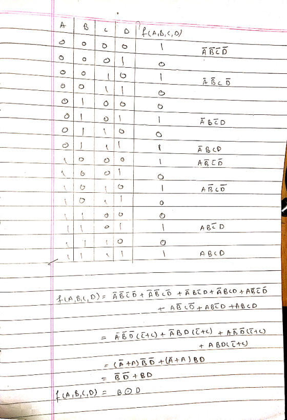
Truth table and the Boolean expression can be verified from the K-map .
 always
I have written SOP for the given K-map.
Q2+Q3
The third circuit in the above image is for Q4 . You haven't mentioned the input but you can get the output from the above circuit anytime for any input. Please consider it.

These are some conversion of any gate to it's equivalent using NAND or NOR gates only.
I have answered all the questions with all the necessary details.
Please rate a thumbs up if satisfied.
Have a nice time ahead :)
Add Answer to:
1 0 0 0 1 10 1. Construct TT and Determine; Boolean expression 2. Draw the...
Name Use SOP, to find Boolean equation for the outputs X, Y, z Construct a logic...
 Name Use SOP, to find Boolean equation for the outputs X, Y, z Construct a logic circuit using AND, OR, and Inverter (NOT) gates which implements the Boolean equations Substitute your logic circuits with NAND gates only, simplify the circuit. 1. 2. 3. Input Outputs A B C 0 0 0 0 0 0 0 0 011 0 0 0
Q2) The following is a Boolean expression of a Combinational Logic Circuit. Construct the truth table...
 Q2) The following is a Boolean expression of a Combinational Logic Circuit. Construct the truth table and a Combinational Logic circuit using AND, OR and NOT logic gates for the Boolean expression. Redraw the logic circuit using only NAND gates. 19 Marks) X = A B C +ABC + ABC
Given the following boolean expression: F = ABC + ABC + ABC 1. Simplify the expression...
 Given the following boolean expression: F = ABC + ABC + ABC 1. Simplify the expression using only NAND operations. 2. Produce a logic diagram implementing the simplified expression using only 2-input NAND gates. 3. Simplify the expression using only NOR operations. 4. Produce a logic diagram implementing the simplified expression using only 2-input NOR gates.
Given the following boolean expression: F=ABC + ABC + ABC 1. Simplify the expression and produce...
 Given the following boolean expression: F=ABC + ABC + ABC 1. Simplify the expression and produce an equivalent operation using only NAND operations. 2. A logic diagram implementing the simplified expression using only inverters and NAND gates.
2. Draw the logic circuit to represent the following Boolean expression using only two input NAND...
 2. Draw the logic circuit to represent the following Boolean expression using only two input NAND gates. F = AB.BC.ĀC
For the given circuit diagram: (1) Obtain the Boolean expression step by step (2) Obtain the...
 For the given circuit diagram: (1) Obtain the Boolean expression step by step (2) Obtain the truth table step by step. (3) From the result of (1) make the truth table of output F and compare with the result of (2) (4) Draw an equivalent circuit for F with fewer NAND gates
Objective: Practice converting a Boolean logic expression into it’s truth table and to show the implementation...
Objective: Practice converting a Boolean logic expression into it’s truth table and to show the implementation of the logic function with hardware logic gates. _ _ Given the Boolean logic expression for output D: A B C + A B C = D In the space below show how you would implement a circuit where the inputs are A, B and C and the output is D with standard logic gates. In the space below assemble the Truth...
X 1. Determine the truth table for the above circuit. A B C 0 0 0...
 X 1. Determine the truth table for the above circuit. A B C 0 0 0 0 0 0 1 0 0 1 1 1 0 0 1 0 1 1 1 0 111 2. Determine the Karnaugh Map for the above circuit and do both an SOP minimization (the left KAI) and a POS minimization (the right KM). Write the minimized Boolean expressions below the corresponding Karnaugh Map BC ВС 00 01 11 10 00 01 11 10 0...
1. Find the Boolean expression of the truth table. Then simplify it and convert it into...
 1. Find the Boolean expression of the truth table. Then simplify it and convert it into the least amount of logic gates possible. AB Output 100 011 101 2. Find the POS form of the Boolean expressions below. Find the truth table and logic minimization method of it. Show its gate level implementation, and show the same gate level implementation using only NAND gates. A(X,Y,Z)= m(0,2,4,6) B(X,Y,2)={m(0,4,5) 3. Create a J-k Flip Flop using a D-Flip Flop. Show its truth...
digital fundamentals thomas floyd Q8. A) Write the SOP (Minterm) Boolean expression for the truth table...
 digital fundamentals thomas floyd
Q8. A) Write the SOP (Minterm) Boolean expression for the truth table in Fig 2 below and draw the logic circuit that will perform the logic in the truth table in. B) Finally implement the same logic circuit by universal gates. [2+2=4] Inputs Output Inputs Output с в А Y C B A Y 0 0 0 0 0 0 0 0 0 1 0 0 1 0 0 0 1 1 1 0 1 1...
digital fundamentals thomas floyd
Q8. A) Write the SOP (Minterm) Boolean expression for the truth table in Fig 2 below and draw the logic circuit that will perform the logic in the truth table in. B) Finally implement the same logic circuit by universal gates. [2+2=4] Inputs Output Inputs Output с в А Y C B A Y 0 0 0 0 0 0 0 0 0 1 0 0 1 0 0 0 1 1 1 0 1 1...
 Name Use SOP, to find Boolean equation for the outputs X, Y, z Construct a logic circuit using AND, OR, and Inverter (NOT) gates which implements the Boolean equations Substitute your logic circuits with NAND gates only, simplify the circuit. 1. 2. 3. Input Outputs A B C 0 0 0 0 0 0 0 0 011 0 0 0
 Q2) The following is a Boolean expression of a Combinational Logic Circuit. Construct the truth table and a Combinational Logic circuit using AND, OR and NOT logic gates for the Boolean expression. Redraw the logic circuit using only NAND gates. 19 Marks) X = A B C +ABC + ABC
 Given the following boolean expression: F = ABC + ABC + ABC 1. Simplify the expression using only NAND operations. 2. Produce a logic diagram implementing the simplified expression using only 2-input NAND gates. 3. Simplify the expression using only NOR operations. 4. Produce a logic diagram implementing the simplified expression using only 2-input NOR gates.
 Given the following boolean expression: F=ABC + ABC + ABC 1. Simplify the expression and produce an equivalent operation using only NAND operations. 2. A logic diagram implementing the simplified expression using only inverters and NAND gates.
 2. Draw the logic circuit to represent the following Boolean expression using only two input NAND gates. F = AB.BC.ĀC
 For the given circuit diagram: (1) Obtain the Boolean expression step by step (2) Obtain the truth table step by step. (3) From the result of (1) make the truth table of output F and compare with the result of (2) (4) Draw an equivalent circuit for F with fewer NAND gates
 X 1. Determine the truth table for the above circuit. A B C 0 0 0 0 0 0 1 0 0 1 1 1 0 0 1 0 1 1 1 0 111 2. Determine the Karnaugh Map for the above circuit and do both an SOP minimization (the left KAI) and a POS minimization (the right KM). Write the minimized Boolean expressions below the corresponding Karnaugh Map BC ВС 00 01 11 10 00 01 11 10 0...
 1. Find the Boolean expression of the truth table. Then simplify it and convert it into the least amount of logic gates possible. AB Output 100 011 101 2. Find the POS form of the Boolean expressions below. Find the truth table and logic minimization method of it. Show its gate level implementation, and show the same gate level implementation using only NAND gates. A(X,Y,Z)= m(0,2,4,6) B(X,Y,2)={m(0,4,5) 3. Create a J-k Flip Flop using a D-Flip Flop. Show its truth...
 digital fundamentals thomas floyd
Q8. A) Write the SOP (Minterm) Boolean expression for the truth table in Fig 2 below and draw the logic circuit that will perform the logic in the truth table in. B) Finally implement the same logic circuit by universal gates. [2+2=4] Inputs Output Inputs Output с в А Y C B A Y 0 0 0 0 0 0 0 0 0 1 0 0 1 0 0 0 1 1 1 0 1 1...
digital fundamentals thomas floyd
Q8. A) Write the SOP (Minterm) Boolean expression for the truth table in Fig 2 below and draw the logic circuit that will perform the logic in the truth table in. B) Finally implement the same logic circuit by universal gates. [2+2=4] Inputs Output Inputs Output с в А Y C B A Y 0 0 0 0 0 0 0 0 0 1 0 0 1 0 0 0 1 1 1 0 1 1...
Most questions answered within 3 hours.
-
Twitter Users and News: A poll conducted in 2013 found that 52%
of U.S. adult Twitter...
asked 14 seconds from now -
How
would I know whether a given amino acid has an ionizable group or
not? please...
asked 7 minutes ago -
True or false?
True False The function of the enzyme acyl CoA
synthetase is the ATP-dependent coupling...
asked 7 minutes ago -
Nadia Corporation adjusts its debt so that its interest coverage
(EBIT/Interest) remains constant at 3. Nadia’s...
asked 9 minutes ago -
In a clinical trial, 20 out of 600 patients taking a
prescription drug complained of flulike...
asked 15 minutes ago -
7. How many types of nuclear processes can produce energy? 8.
How many types of radioactive...
asked 19 minutes ago -
For both the Sn2 and Sn1 reaction
conditions:
Structure | Rxn (Y/N) at room T° Rxn...
asked 19 minutes ago -
11. In cell N2, enter a formula using the IF function and a
structured reference to...
asked 19 minutes ago -
There is X-linked mutations in flies in this example. You need
to determine the inheritence pattern...
asked 21 minutes ago -
1) There is a 5.0 μC charge at each of 3 corners of a square
(each...
asked 32 minutes ago -
A study of 420,095 cell phone users found that
134 of them developed cancer of the...
asked 36 minutes ago -
2.50 g of NH4Cl is added to 12.9 g of water. Calculate the
molality of the...
asked 38 minutes ago