
Homework Answers

Add Answer to:
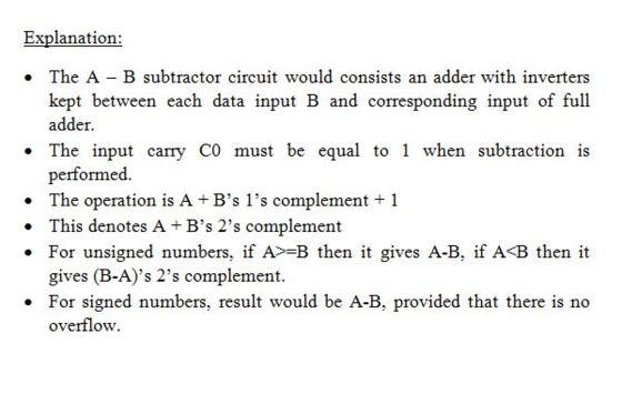
In this problem, you will design a 4-bit 2's complement sub tractor, implement it in Logic...
number 4 and 5 please! PROBLEM STATEMENT A logic circuit is needed to add multi-bit binary...
 number 4 and 5 please!
PROBLEM STATEMENT A logic circuit is needed to add multi-bit binary numbers. A 2-level circuit that would add two four-bit numbers would have 9 inputs and five outputs. Although a 2-level SOP or POS circuit theoretically would be very fast, it has numerous drawbacks that make it impractical. The design would be very complex in terms of the number of logic gates. The number of inputs for each gate would challenge target technologies. Testing would...
number 4 and 5 please!
PROBLEM STATEMENT A logic circuit is needed to add multi-bit binary numbers. A 2-level circuit that would add two four-bit numbers would have 9 inputs and five outputs. Although a 2-level SOP or POS circuit theoretically would be very fast, it has numerous drawbacks that make it impractical. The design would be very complex in terms of the number of logic gates. The number of inputs for each gate would challenge target technologies. Testing would...
Design a logic circuit that provides the 2's complement of a 4 bit binary number using...
Design a logic circuit that provides the 2's complement of a 4 bit binary number using adders. Please write the truth table and draw the gate level schematic for it.
Please design and implement a combinational circuit called 4-bit adder to add two 4-bit binary numbers,...
Please design and implement a combinational circuit called 4-bit adder to add two 4-bit binary numbers, e.g. 1011 + 1110 = 1 1 0 0 1, the 5-bit result is 1 1 0 0 1 in which the leftmost bit is carry-out bit and sum result is 1 0 0 1, so that final sum is 1 1 0 0 1 which is 25 in decimal. (b) Design and Implement the four-bit adder circuit preferably using CEDAR logic simulator...
Design a sequential circuit that outputs 2’s complement of a bit sequence. The bit sequence will...
Design a sequential circuit that outputs 2’s complement of a bit sequence. The bit sequence will be given to the circuit in reverse order. For instance, if the given bit sequence is 0010101000, the circuit should output 1101011000.
8.9 Use FA's to design a device which will calculate 5x +4y where x and y are 4-bit unsigned inpu...
 8.9 Use FA's to design a device which will calculate 5x +4y where x and y are 4-bit unsigned inputs. Use 8-bit arithmetic. 8.10 Use FA's and logic gates to design a device which will multiply a given 4-bit signed input by -2. (Hint: if you think about this for a bit, you should see the answer is actually pretty straightforward. ..) in addition to the normal sum and carry outputs, a third output called overflow does not. 8.11 Use...
1 Design an arithmetic-logic circuit with 3-bit opcode variables P Pila and two 4-bits data inputs...
 1 Design an arithmetic-logic circuit with 3-bit opcode variables P Pila and two 4-bits data inputs A and B. The circuit generates the following arithmetic, and logic operations. Draw the logic diagram with carry COLL) and overflow (OF )outputs. (Using a 4-bit adder) Р 1 2 P2 0 0 P. 0 0 1 1 A A A. A Q Q Q 0 1 0 OPERATION A - B A + B A A +1 AAB A A/ 2 A* 2...
Problem 3 - Arithmetie Logic Unit (ALU) Design us poins Design a 4-bit ALU that has two selection...
 Problem 3 - Arithmetie Logic Unit (ALU) Design us poins Design a 4-bit ALU that has two selection variables Si Design an optimized circuit (mus external gates for circuit B operates based on the function table given below. The arithmetic unit and So and generates the arithmetic operations given below. and generatest Use a 4-1 MUX block with Si So Cin = 1 F-A (complement) F = A+B (add) FB (transfer) F A+B F = A+ 1 (negate) F A+B+...
Introduction: This experiment studies the design of an 8-bit adder/subtractor circuit using VHDL capture. The experiment...
 Introduction: This experiment studies the design of an 8-bit adder/subtractor circuit using VHDL capture. The experiment investigates the implementation of addition and subtraction operations with circuits. This lab uses the virtual simulation environment to validate the design practically in the FPGA board. Equipment: • This experiment requires Quartus Prime and the Intel's DE2-115 FPGA board. • All students should have the Intel QP and ModelSim-Intel-Starter-Edition softwares installed in personal computers. • VPN connection to UNB Network and remote desktop software...
You need to design a circuit that implements the functions in the following table: S0 and...
 You need to design a circuit that implements the functions in
the following table:
S0 and S1 are 1-bit control inputs to select the function of the
circuit. Inputs A and B are 4-bit numbers in 2s complement form.
The output is also a 4-bit number in 2s complement form. You are
allowed to use only one TTL 7483 4-bit adder to implement all the
functions. But any number of other components (except the adder)
can be used.
HINT: Design...
You need to design a circuit that implements the functions in
the following table:
S0 and S1 are 1-bit control inputs to select the function of the
circuit. Inputs A and B are 4-bit numbers in 2s complement form.
The output is also a 4-bit number in 2s complement form. You are
allowed to use only one TTL 7483 4-bit adder to implement all the
functions. But any number of other components (except the adder)
can be used.
HINT: Design...
Tim Question 1 Atte 20 pts 2H 24 Design a 1-bit Full Adder using NOR gates...
 Tim Question 1 Atte 20 pts 2H 24 Design a 1-bit Full Adder using NOR gates only, you must include and show: Truth tables, detail logic gate circuit designs, and Boolean expressions Upload Choose a File 20 pts Question 2 Design a 4-bit Full Adder with inputs (Xo...X3, Yo...Y3) in which inputs X are connect to two 4-bit registers via four 2-to-1 Multiplexers and inputs Y are connected to two other 4-bit registers via four 2-to-1 Multiplexers. In this case...
 number 4 and 5 please!
PROBLEM STATEMENT A logic circuit is needed to add multi-bit binary numbers. A 2-level circuit that would add two four-bit numbers would have 9 inputs and five outputs. Although a 2-level SOP or POS circuit theoretically would be very fast, it has numerous drawbacks that make it impractical. The design would be very complex in terms of the number of logic gates. The number of inputs for each gate would challenge target technologies. Testing would...
number 4 and 5 please!
PROBLEM STATEMENT A logic circuit is needed to add multi-bit binary numbers. A 2-level circuit that would add two four-bit numbers would have 9 inputs and five outputs. Although a 2-level SOP or POS circuit theoretically would be very fast, it has numerous drawbacks that make it impractical. The design would be very complex in terms of the number of logic gates. The number of inputs for each gate would challenge target technologies. Testing would...
 8.9 Use FA's to design a device which will calculate 5x +4y where x and y are 4-bit unsigned inputs. Use 8-bit arithmetic. 8.10 Use FA's and logic gates to design a device which will multiply a given 4-bit signed input by -2. (Hint: if you think about this for a bit, you should see the answer is actually pretty straightforward. ..) in addition to the normal sum and carry outputs, a third output called overflow does not. 8.11 Use...
 1 Design an arithmetic-logic circuit with 3-bit opcode variables P Pila and two 4-bits data inputs A and B. The circuit generates the following arithmetic, and logic operations. Draw the logic diagram with carry COLL) and overflow (OF )outputs. (Using a 4-bit adder) Р 1 2 P2 0 0 P. 0 0 1 1 A A A. A Q Q Q 0 1 0 OPERATION A - B A + B A A +1 AAB A A/ 2 A* 2...
 Problem 3 - Arithmetie Logic Unit (ALU) Design us poins Design a 4-bit ALU that has two selection variables Si Design an optimized circuit (mus external gates for circuit B operates based on the function table given below. The arithmetic unit and So and generates the arithmetic operations given below. and generatest Use a 4-1 MUX block with Si So Cin = 1 F-A (complement) F = A+B (add) FB (transfer) F A+B F = A+ 1 (negate) F A+B+...
 Introduction: This experiment studies the design of an 8-bit adder/subtractor circuit using VHDL capture. The experiment investigates the implementation of addition and subtraction operations with circuits. This lab uses the virtual simulation environment to validate the design practically in the FPGA board. Equipment: • This experiment requires Quartus Prime and the Intel's DE2-115 FPGA board. • All students should have the Intel QP and ModelSim-Intel-Starter-Edition softwares installed in personal computers. • VPN connection to UNB Network and remote desktop software...
 You need to design a circuit that implements the functions in
the following table:
S0 and S1 are 1-bit control inputs to select the function of the
circuit. Inputs A and B are 4-bit numbers in 2s complement form.
The output is also a 4-bit number in 2s complement form. You are
allowed to use only one TTL 7483 4-bit adder to implement all the
functions. But any number of other components (except the adder)
can be used.
HINT: Design...
You need to design a circuit that implements the functions in
the following table:
S0 and S1 are 1-bit control inputs to select the function of the
circuit. Inputs A and B are 4-bit numbers in 2s complement form.
The output is also a 4-bit number in 2s complement form. You are
allowed to use only one TTL 7483 4-bit adder to implement all the
functions. But any number of other components (except the adder)
can be used.
HINT: Design...
 Tim Question 1 Atte 20 pts 2H 24 Design a 1-bit Full Adder using NOR gates only, you must include and show: Truth tables, detail logic gate circuit designs, and Boolean expressions Upload Choose a File 20 pts Question 2 Design a 4-bit Full Adder with inputs (Xo...X3, Yo...Y3) in which inputs X are connect to two 4-bit registers via four 2-to-1 Multiplexers and inputs Y are connected to two other 4-bit registers via four 2-to-1 Multiplexers. In this case...
Most questions answered within 3 hours.
-
A sample of 24 observations is selected from a normal population
where the sample standard deviation...
asked 3 minutes ago -
How social media will be used in education in 2030?? Actually i
am working on an...
asked 5 minutes ago -
Using Horner's scheme, represent (evaluate) the 2's complement
number 10011101 in decimal.
CAUTION: You will earn...
asked 7 minutes ago -
The vapor pressure of ethanol at 34.7 degrees Celsius is
100mmHg, and Hvap= 38.6 kJ/mol. What...
asked 9 minutes ago -
#3
Given the following hypotheses:
H0: μ = 520
H1: μ ≠ 520
A random sample...
asked 22 minutes ago -
You have been given a stipend to expand your “troubleshooting
tool kit” by adding three additional...
asked 17 minutes ago -
A machine costs P320,000 with a scrap value of 10% of the
original price at the...
asked 19 minutes ago -
Suppose that you have a reflection diffraction grating with n=
140 lines per millimeter. Light from...
asked 22 minutes ago -
A physician at a large clinic sees clients of all ages: babies
(<2 years old, event...
asked 26 minutes ago -
Find the indicated area under the standard normal curve. To the
right of zequals 1.16Find the...
asked 26 minutes ago -
When a student misses one of the scheduled class sessions, I
know for certain that...
the...
asked 33 minutes ago -
Del Gato Clinic's cash account shows a $14,164 debit balance and
its bank statement shows $13,947...
asked 34 minutes ago