
Homework Answers
The circuit given in the Question is "RC Low Pass Filter" of "First Order" as there is only one load component present which is 'Capacitor' , and then by using KVL property the differential equation is calculated and by observing first order differential equation the 'Time constant' and 'static sensitivity (K) ' is calculated and then by using Charging equation of capacitor the 'elapsed time' is calculated.
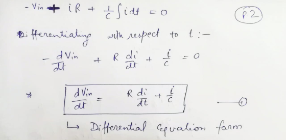
there are 6 different pictures in the solution ,so for complete solution download all(6) pictures.


![» 0.95 Vin = Vin {i- é t/Re] * 0.95 = -e-tipe * etike -0.05 taking log both side :- t e = ln (0.05) ata RC [-2.996] t= RC *](http://img.homeworklib.com/questions/e7c7bf30-8067-11eb-b370-b76479cee33f.png?x-oss-process=image/resize,w_560)
Add Answer to:
Problem 1. (40 pts): A student in ME 345 shows you the following circuit with R=1.0...
Objective Integrate material from Lecture 2 into practical problem. The circuit below shows a filter commonly...
 Objective Integrate material from Lecture 2 into practical problem. The circuit below shows a filter commonly used as the output stage of a switch mode power supply. In a switch mode power supply, Vin() is switched between 0 and the DC input supply voltage, in this case 12V. The filter smooths the switched input so that it is close to DC at the desired output level (see figure below circuit). The desired output level is set by controlling the proportion...
Problem 5: (20 points) Given the following circuit VIN L Vout R a) Write the loop...
 Problem 5: (20 points) Given the following circuit VIN L Vout R a) Write the loop equation for the circuit, and then find the transfer function Vout(s) H(S) = Express H(s) so that the coefficient of the s in the denominator is 1. Vin(s) b) If Vin(t) is 20u(t), find out(t). c) If Vin(t) is 20u(t) find the final value using the final value theorem (show your work), d) Assume (R/L) = 10, if the input is Vin(t) = 100...
Part I: Inverting Amplifier Procedure: 1. Build the circuit model for inverting amplifier in PSpice with...
 Part I: Inverting Amplifier Procedure: 1. Build the circuit model for inverting amplifier in PSpice with the following parameters: Ri = 5 k 2, R2 = 20 ks2, V+ = 10 V, V-=-10 V. 2. Hand calculates the theoretical closed loop gain Vout/Vin of the circuit model. 3. Generate a triangular waveform for Vin with the amplitude of 1 V and the period of 1 ms. 4. Run simulation. a. Set circuit model parameters. i.e., for voltage source: click VPWL...
Prelab Preparation: For the RC circuit shown in Figure 1, derive the modeling equation relating the output volta ge...
 Prelab Preparation: For the RC circuit shown in Figure 1, derive the modeling equation relating the output volta ge Vout to the input voltage vin. What is the transfer function? What is the time constant of the system? Vout Figure 1: RC Circuit What is the analytical step response solution in terms of vin, Rand C? For assumed values of R 1 K, and C 6.8 uF, perform a simulation using Matlab/Simulink assuming an input square wave signal of 5Vpp,...
Problem 24: (18 points) 1. (6 points) Figure 2 shows an RC circuit with input f(t)...
 Problem 24: (18 points) 1. (6 points) Figure 2 shows an RC circuit with input f(t) and output y(t) Function Generator R, v, (r) y1) Figure 2: RC circuit. (a) (1 point) Sketch the circuit in the phasor domain by replacing the capacitor with its impedance represen- (b) (3 points) Using circuit analysis techniques, show that the frequency response function is Specify the DC gain, K, and the time constant, T, in terms of the parameters R, R, and C...
I need help with numbers 4,6,7,8,9 please? 12 VDC 1.0 k ohms 10k ohms C3 1.0 uF C1 1.0 UF , R Load Baca 1 80 10k ohns 300 mVp-p 1.0 kHz 100 ohms .7k ohms C2 47uF 330 ohms 4. Calculate the following pa...
 I need help with numbers 4,6,7,8,9 please?
12 VDC 1.0 k ohms 10k ohms C3 1.0 uF C1 1.0 UF , R Load Baca 1 80 10k ohns 300 mVp-p 1.0 kHz 100 ohms .7k ohms C2 47uF 330 ohms 4. Calculate the following parameters assuming capacitor C2 has been removed from the circuit with the 1.0k2 resistor as the load. RIN BASE Av Vour 5. Construct the circuit shown on the previous page. Before connecting the AC supply, measure...
I need help with numbers 4,6,7,8,9 please?
12 VDC 1.0 k ohms 10k ohms C3 1.0 uF C1 1.0 UF , R Load Baca 1 80 10k ohns 300 mVp-p 1.0 kHz 100 ohms .7k ohms C2 47uF 330 ohms 4. Calculate the following parameters assuming capacitor C2 has been removed from the circuit with the 1.0k2 resistor as the load. RIN BASE Av Vour 5. Construct the circuit shown on the previous page. Before connecting the AC supply, measure...
Problem 4 (50 pts): Consider the electrical circuit represented in figure, with R = 102, C...
 Problem 4 (50 pts): Consider the electrical circuit represented in figure, with R = 102, C = 1 F and L=1 H. Assume V (t) as input and i(t) as output E ER V.(t) a) (5 pts) Determine the differential equation of the system b) (5 pts) Find the transfer function of the system c) (20 pts) Write the symbolic expressions of magnitude and phase of the transfer function d) (20 pts) Determine the expression of steady-state response of the...
1. Figure 1 shows a CE power amplifier in which the collector resistor serves also as...
 1. Figure 1 shows a CE power amplifier in which the collector resistor serves also as the load resistor. Assume Bpc Bac 100 a. Determine the dc Q-point (lco and VCEQ). b. Determine the voltage gain and the power gain c. The power dissipated in the transistor with no load. d. The total power from the power supply with no load e. The signal power in the load with a 500 mV input. f. What changes would be necessary to...
1-Clear handwriting 2-Correct answer 3-Organized 4-answer all the questions Please Problem 2 On the circuit on...
 1-Clear handwriting
2-Correct answer
3-Organized
4-answer all the questions
Please
Problem 2 On the circuit on Figure P2, transi stor Q1 has a threshold voltage of Vt = 2 V and a transconductance parameter of k = 100 mA/V2. Note that Vcc = -Vee = 4.5 V. Moreover, capacitors C1, C2, and C3 can be assumed to be very large VDD 4.5.0 R3 25kQ R1 300kn C2 Vout C1 Rsig Q1 1k0 R2 200kn Vsig (R4 2kQ C3 -4.5V VSS...
1-Clear handwriting
2-Correct answer
3-Organized
4-answer all the questions
Please
Problem 2 On the circuit on Figure P2, transi stor Q1 has a threshold voltage of Vt = 2 V and a transconductance parameter of k = 100 mA/V2. Note that Vcc = -Vee = 4.5 V. Moreover, capacitors C1, C2, and C3 can be assumed to be very large VDD 4.5.0 R3 25kQ R1 300kn C2 Vout C1 Rsig Q1 1k0 R2 200kn Vsig (R4 2kQ C3 -4.5V VSS...
please answer C,D,E Consider the electrical circuit shown in Fig.1. Assume switch S remain at position...
 please answer C,D,E
Consider the electrical circuit shown in Fig.1. Assume switch S remain at position 1 for longer time and at t = 0 the switch is moved to position 2 from position 1. t=0 4 ΚΩ 1S v(t) i(t) m А 2 12 V 100 uF 8 ΚΩ Fig.3 Diagram for Q2 a) What is the initial capacitor voltage v(0-), before it move to position 2 [20 marks) b) Soon after the switch is moved to position 2...
please answer C,D,E
Consider the electrical circuit shown in Fig.1. Assume switch S remain at position 1 for longer time and at t = 0 the switch is moved to position 2 from position 1. t=0 4 ΚΩ 1S v(t) i(t) m А 2 12 V 100 uF 8 ΚΩ Fig.3 Diagram for Q2 a) What is the initial capacitor voltage v(0-), before it move to position 2 [20 marks) b) Soon after the switch is moved to position 2...
 Objective Integrate material from Lecture 2 into practical problem. The circuit below shows a filter commonly used as the output stage of a switch mode power supply. In a switch mode power supply, Vin() is switched between 0 and the DC input supply voltage, in this case 12V. The filter smooths the switched input so that it is close to DC at the desired output level (see figure below circuit). The desired output level is set by controlling the proportion...
 Problem 5: (20 points) Given the following circuit VIN L Vout R a) Write the loop equation for the circuit, and then find the transfer function Vout(s) H(S) = Express H(s) so that the coefficient of the s in the denominator is 1. Vin(s) b) If Vin(t) is 20u(t), find out(t). c) If Vin(t) is 20u(t) find the final value using the final value theorem (show your work), d) Assume (R/L) = 10, if the input is Vin(t) = 100...
 Part I: Inverting Amplifier Procedure: 1. Build the circuit model for inverting amplifier in PSpice with the following parameters: Ri = 5 k 2, R2 = 20 ks2, V+ = 10 V, V-=-10 V. 2. Hand calculates the theoretical closed loop gain Vout/Vin of the circuit model. 3. Generate a triangular waveform for Vin with the amplitude of 1 V and the period of 1 ms. 4. Run simulation. a. Set circuit model parameters. i.e., for voltage source: click VPWL...
 Prelab Preparation: For the RC circuit shown in Figure 1, derive the modeling equation relating the output volta ge Vout to the input voltage vin. What is the transfer function? What is the time constant of the system? Vout Figure 1: RC Circuit What is the analytical step response solution in terms of vin, Rand C? For assumed values of R 1 K, and C 6.8 uF, perform a simulation using Matlab/Simulink assuming an input square wave signal of 5Vpp,...
 Problem 24: (18 points) 1. (6 points) Figure 2 shows an RC circuit with input f(t) and output y(t) Function Generator R, v, (r) y1) Figure 2: RC circuit. (a) (1 point) Sketch the circuit in the phasor domain by replacing the capacitor with its impedance represen- (b) (3 points) Using circuit analysis techniques, show that the frequency response function is Specify the DC gain, K, and the time constant, T, in terms of the parameters R, R, and C...
 I need help with numbers 4,6,7,8,9 please?
12 VDC 1.0 k ohms 10k ohms C3 1.0 uF C1 1.0 UF , R Load Baca 1 80 10k ohns 300 mVp-p 1.0 kHz 100 ohms .7k ohms C2 47uF 330 ohms 4. Calculate the following parameters assuming capacitor C2 has been removed from the circuit with the 1.0k2 resistor as the load. RIN BASE Av Vour 5. Construct the circuit shown on the previous page. Before connecting the AC supply, measure...
I need help with numbers 4,6,7,8,9 please?
12 VDC 1.0 k ohms 10k ohms C3 1.0 uF C1 1.0 UF , R Load Baca 1 80 10k ohns 300 mVp-p 1.0 kHz 100 ohms .7k ohms C2 47uF 330 ohms 4. Calculate the following parameters assuming capacitor C2 has been removed from the circuit with the 1.0k2 resistor as the load. RIN BASE Av Vour 5. Construct the circuit shown on the previous page. Before connecting the AC supply, measure...
 Problem 4 (50 pts): Consider the electrical circuit represented in figure, with R = 102, C = 1 F and L=1 H. Assume V (t) as input and i(t) as output E ER V.(t) a) (5 pts) Determine the differential equation of the system b) (5 pts) Find the transfer function of the system c) (20 pts) Write the symbolic expressions of magnitude and phase of the transfer function d) (20 pts) Determine the expression of steady-state response of the...
 1. Figure 1 shows a CE power amplifier in which the collector resistor serves also as the load resistor. Assume Bpc Bac 100 a. Determine the dc Q-point (lco and VCEQ). b. Determine the voltage gain and the power gain c. The power dissipated in the transistor with no load. d. The total power from the power supply with no load e. The signal power in the load with a 500 mV input. f. What changes would be necessary to...
 1-Clear handwriting
2-Correct answer
3-Organized
4-answer all the questions
Please
Problem 2 On the circuit on Figure P2, transi stor Q1 has a threshold voltage of Vt = 2 V and a transconductance parameter of k = 100 mA/V2. Note that Vcc = -Vee = 4.5 V. Moreover, capacitors C1, C2, and C3 can be assumed to be very large VDD 4.5.0 R3 25kQ R1 300kn C2 Vout C1 Rsig Q1 1k0 R2 200kn Vsig (R4 2kQ C3 -4.5V VSS...
1-Clear handwriting
2-Correct answer
3-Organized
4-answer all the questions
Please
Problem 2 On the circuit on Figure P2, transi stor Q1 has a threshold voltage of Vt = 2 V and a transconductance parameter of k = 100 mA/V2. Note that Vcc = -Vee = 4.5 V. Moreover, capacitors C1, C2, and C3 can be assumed to be very large VDD 4.5.0 R3 25kQ R1 300kn C2 Vout C1 Rsig Q1 1k0 R2 200kn Vsig (R4 2kQ C3 -4.5V VSS...
 please answer C,D,E
Consider the electrical circuit shown in Fig.1. Assume switch S remain at position 1 for longer time and at t = 0 the switch is moved to position 2 from position 1. t=0 4 ΚΩ 1S v(t) i(t) m А 2 12 V 100 uF 8 ΚΩ Fig.3 Diagram for Q2 a) What is the initial capacitor voltage v(0-), before it move to position 2 [20 marks) b) Soon after the switch is moved to position 2...
please answer C,D,E
Consider the electrical circuit shown in Fig.1. Assume switch S remain at position 1 for longer time and at t = 0 the switch is moved to position 2 from position 1. t=0 4 ΚΩ 1S v(t) i(t) m А 2 12 V 100 uF 8 ΚΩ Fig.3 Diagram for Q2 a) What is the initial capacitor voltage v(0-), before it move to position 2 [20 marks) b) Soon after the switch is moved to position 2...
Most questions answered within 3 hours.
-
Choose the sentence that uses correct punctuation.
1a. The prefatory parts of a report include the...
asked 3 minutes ago -
For the element arsenic, which one of the following sets of
quantum numbers could not apply...
asked 13 minutes ago -
Compare and contrast the architectures of 3 types of ADCs:
Flash, SAR, and pipelined. Use the...
asked 14 minutes ago -
Given P(A) = 0.40, P(B) = 0.50, P(A ∩ B) = 0.15. Which of the
following...
asked 18 minutes ago -
Explain changes in workforce participation for women with
children. What legislation exists related to work and...
asked 20 minutes ago -
How high must a pointed arch be if it is to span a
space 4.2 m...
asked 25 minutes ago -
A housepainter who weighs 750 N stands 0.6 m from one end of a
2.0 m...
asked 27 minutes ago -
Implement Singly Linked List detectLoop in Java.
It would check whether the linked list contains a...
asked 30 minutes ago -
A small mailbag is released from a helicopter that is descending
steadily at 2.10 m/s.
After...
asked 31 minutes ago -
Write a C – program that calls a user-defined function from
within main() that determines the...
asked 35 minutes ago -
For a 2-Level design, with 8 factors, a recommended screening
design model is:
a. Taguchi L12...
asked 1 hour ago -
1. Define a function in python that returns the sum of the
following 4 lists. Remember...
asked 1 hour ago