
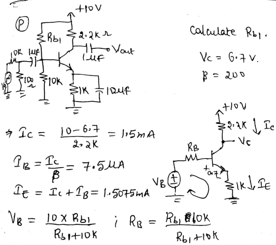
Figure 1 is a common-emitter amplifier (with input divider). Calculate the base resistance Rb1 that is needed to bias the device at a collector voltage of Vc≈ 6-7 V. Assume a nominal value of β≈ 200 for this calculation.
Homework Answers

Add Answer to:
Figure 1 is a common-emitter amplifier (with input divider).
Calculate the base resistance Rb1 that is...
Shown below is a single stage common emitter amplifier with a unipolar dc power supply using an 2...
 Shown below is a single stage common emitter amplifier with a unipolar dc power supply using an 2N3904 NPN BJT as the active device. It is specified that V+ 40 V, C1 C2CE 100uF, Ro-7.5 k2, REi-5.1kS2, and Ri - 36k52. Design the circuit so that the dc collector current is 2 mA and the magnitude of the small-signal midband voltage gain is 32.3. For the design calculations assume that the base-to- emitter dc voltage drop is 0.65 V, the...
FIND THE VALUES OF Rb1, Rb2, Re,Rc, rin , rout, overall gain and open circuit gain First, design a common emitter BJT a...
 FIND THE VALUES OF Rb1, Rb2, Re,Rc, rin , rout, overall gain and
open circuit gain
First, design a common emitter BJT amplifier Second, analyze the amplifier.( Avo, Gv, Rin, Rout) Third, compare your calculation with Multisim. Report must include comparison between your calculation & simulation results overall voltage gain, open circuit voltage gain, input resistance, and output resistance. This design project is not group work, must be done individually. Type your report. Design a discrete common emitter BJT amplifier.(Determine...
FIND THE VALUES OF Rb1, Rb2, Re,Rc, rin , rout, overall gain and
open circuit gain
First, design a common emitter BJT amplifier Second, analyze the amplifier.( Avo, Gv, Rin, Rout) Third, compare your calculation with Multisim. Report must include comparison between your calculation & simulation results overall voltage gain, open circuit voltage gain, input resistance, and output resistance. This design project is not group work, must be done individually. Type your report. Design a discrete common emitter BJT amplifier.(Determine...
Can I get help with part g through part r, please? Given the following Common-Emitter Amplifier...
 Can I get help with part g through part r, please?
Given the following Common-Emitter Amplifier with Voltage-Divider Bias: The transistor is a Silicon device with B160 (Beta 160) and transistor r.= 30 kn: 20 V 34.7k LAL = Vou 35.10 31.1k LRE $3900 03 - Find the following quantities in parts a through where means Quiescent DC): a) Thevenin Voltage and Thevenin Resistance Re b) Base Current la Collector Current le d) Emitter Current le e) Transistor Collector-Emitter Quiescent...
Can I get help with part g through part r, please?
Given the following Common-Emitter Amplifier with Voltage-Divider Bias: The transistor is a Silicon device with B160 (Beta 160) and transistor r.= 30 kn: 20 V 34.7k LAL = Vou 35.10 31.1k LRE $3900 03 - Find the following quantities in parts a through where means Quiescent DC): a) Thevenin Voltage and Thevenin Resistance Re b) Base Current la Collector Current le d) Emitter Current le e) Transistor Collector-Emitter Quiescent...
For the cascade amplifier of Figure Q1(a), determine the (1) transconductance factor, gm. a.c. diode resistance.,...
 For the cascade amplifier of Figure Q1(a), determine the (1) transconductance factor, gm. a.c. diode resistance., re. (iii) ac equivalent circuit (iv) input impedance, Z (v) output impedance, Z. (vi) voltage gain, Avi (vii) voltage gain, Av2. (viii) total cascade voltage gain, Avr. Given gm = 21 pss lvpl + 15 V Ipss - 10 mA Vp.4V Vase -- 1.5 V βος = 50 μs Γ. 40 ΚΩ RO 3.3 ΚΩ R81 22 ΚΩ Rc 10 ΚΩ O V. β...
1. Design the common-emitter amplifier in Fig. 4(a) with the following specifications: Supply Vol...
 Figure 4. (a)
1. Design the common-emitter amplifier in Fig. 4(a) with the following specifications: Supply Voltage, Vcc 0-to-Peak Output Swing, V Voltage Gain, A. Input Resistance, R Output Resistance, Ro THD for 5kHz 1 V (0-to-peak) Sine Wave Output Voltage, V Relative Variation of Ic for VBE 0.7t 0.1V Transistor's Current Gain, β 5V 25 1.8kS2 4% 10% 100 Show your design procedure and all your calculations. Your design should be insensitive to B variations. Vcc RB1 Rc 0...
Figure 4. (a)
1. Design the common-emitter amplifier in Fig. 4(a) with the following specifications: Supply Voltage, Vcc 0-to-Peak Output Swing, V Voltage Gain, A. Input Resistance, R Output Resistance, Ro THD for 5kHz 1 V (0-to-peak) Sine Wave Output Voltage, V Relative Variation of Ic for VBE 0.7t 0.1V Transistor's Current Gain, β 5V 25 1.8kS2 4% 10% 100 Show your design procedure and all your calculations. Your design should be insensitive to B variations. Vcc RB1 Rc 0...
Solve for the following using: 1) exact method 2) approximate method compare if approximate method is...
 Solve for the following using:
1) exact method
2) approximate method
compare if approximate method is sufficient for analysis. which
solution is better?
Example For the voltage divider bias circuit, RB1-13K2, R 2.2k2 , Rc-68K(2. RE-1.5K(2.Vcc-15 V. VCEsat -0.3 V and β of the Si transistor is 80. Determine the following O" (a) DC base voltage and DC emitter voltage of the transistor amplifier (b) DC operating voltages and currents of the transistor amplifier (lBo, Ico, IEo and VcEO) (c)...
Solve for the following using:
1) exact method
2) approximate method
compare if approximate method is sufficient for analysis. which
solution is better?
Example For the voltage divider bias circuit, RB1-13K2, R 2.2k2 , Rc-68K(2. RE-1.5K(2.Vcc-15 V. VCEsat -0.3 V and β of the Si transistor is 80. Determine the following O" (a) DC base voltage and DC emitter voltage of the transistor amplifier (b) DC operating voltages and currents of the transistor amplifier (lBo, Ico, IEo and VcEO) (c)...
1. For the cascade amplifier of the figure, calculate the polarization voltages and current colle...
 For the cascade amplifier of the figure, calculate the
polarization voltages
Please clarity answer, thanks!!
1. For the cascade amplifier of the figure, calculate the polarization voltages and current collector of each stage. Also, calculate the voltage gain for each stage and the total voltage gain for cascade amplifier. 2. Repeat the previous steps using a load resistance of 2.2 kΩ 3. Calculate the input and output impedances for the cascade amplifier and the cutoff frequencies (fi) for the cascade...
For the cascade amplifier of the figure, calculate the
polarization voltages
Please clarity answer, thanks!!
1. For the cascade amplifier of the figure, calculate the polarization voltages and current collector of each stage. Also, calculate the voltage gain for each stage and the total voltage gain for cascade amplifier. 2. Repeat the previous steps using a load resistance of 2.2 kΩ 3. Calculate the input and output impedances for the cascade amplifier and the cutoff frequencies (fi) for the cascade...
Example 6-5 & 6-6 page 284 Calculate the base-to-collector voltage gain of the amplifier in the f...
 Example 6-5 & 6-6 page 284 Calculate the base-to-collector voltage gain of the amplifier in the figure below both without and with an emitter bypass capacitor if there is no load resistor +12V Rc C3 22 ㏀ 2N3904 v- Calculate the base-to-collector voltage gain of the amplifier when a load resistance of 5K2 is connected to the output .The emitter is effectively bypassed and r 6.582 R2 6.8 kΩ 560 Ω
Example 6-5 & 6-6 page 284 Calculate the base-to-collector...
Example 6-5 & 6-6 page 284 Calculate the base-to-collector voltage gain of the amplifier in the figure below both without and with an emitter bypass capacitor if there is no load resistor +12V Rc C3 22 ㏀ 2N3904 v- Calculate the base-to-collector voltage gain of the amplifier when a load resistance of 5K2 is connected to the output .The emitter is effectively bypassed and r 6.582 R2 6.8 kΩ 560 Ω
Example 6-5 & 6-6 page 284 Calculate the base-to-collector...
Perform a simple initial design of an ac coupled common-emitter amplifier with four resistor biasing and emitter by-pass...
 Perform a simple initial design of an ac coupled common-emitter
amplifier with
four resistor biasing and emitter by-pass capacitor, to have a
voltage gain of about
100, for the following conditions. Justify any approximations used.
(Assume Ic=1/300 A)
i)Transistor ac common-emitter gain, B, 100 ii) Supply voltage ofV0c-20V iii) Allow 10% Vcc across RE DC collector voltage of 10 V iv) v) DC current in the base bias resistors should be ten times greater than the DC base current. Assume...
Perform a simple initial design of an ac coupled common-emitter
amplifier with
four resistor biasing and emitter by-pass capacitor, to have a
voltage gain of about
100, for the following conditions. Justify any approximations used.
(Assume Ic=1/300 A)
i)Transistor ac common-emitter gain, B, 100 ii) Supply voltage ofV0c-20V iii) Allow 10% Vcc across RE DC collector voltage of 10 V iv) v) DC current in the base bias resistors should be ten times greater than the DC base current. Assume...
1.0 kn. RE-390 Ω, r-15 Ω. and ßac-75. 5. For a common-emitter amplifier, Rc Assuming that Rg is completely bypassed at the operating frequency, the voltage gain is (a) 66.7 (d) 75 (b) 2.56 (c) 2....
 1.0 kn. RE-390 Ω, r-15 Ω. and ßac-75. 5. For a common-emitter amplifier, Rc Assuming that Rg is completely bypassed at the operating frequency, the voltage gain is (a) 66.7 (d) 75 (b) 2.56 (c) 2.47 6. In the circuit of Question 5, if the frequency is reduced to the point where Xctbypass) RE, the voltage gain (a) remains the same (b) is less (c) is greater 7. In a common-emitter amplifier with voltage-divider bias, Rimlbase) 68 k2, Ri 33...
 Shown below is a single stage common emitter amplifier with a unipolar dc power supply using an 2N3904 NPN BJT as the active device. It is specified that V+ 40 V, C1 C2CE 100uF, Ro-7.5 k2, REi-5.1kS2, and Ri - 36k52. Design the circuit so that the dc collector current is 2 mA and the magnitude of the small-signal midband voltage gain is 32.3. For the design calculations assume that the base-to- emitter dc voltage drop is 0.65 V, the...
 FIND THE VALUES OF Rb1, Rb2, Re,Rc, rin , rout, overall gain and
open circuit gain
First, design a common emitter BJT amplifier Second, analyze the amplifier.( Avo, Gv, Rin, Rout) Third, compare your calculation with Multisim. Report must include comparison between your calculation & simulation results overall voltage gain, open circuit voltage gain, input resistance, and output resistance. This design project is not group work, must be done individually. Type your report. Design a discrete common emitter BJT amplifier.(Determine...
FIND THE VALUES OF Rb1, Rb2, Re,Rc, rin , rout, overall gain and
open circuit gain
First, design a common emitter BJT amplifier Second, analyze the amplifier.( Avo, Gv, Rin, Rout) Third, compare your calculation with Multisim. Report must include comparison between your calculation & simulation results overall voltage gain, open circuit voltage gain, input resistance, and output resistance. This design project is not group work, must be done individually. Type your report. Design a discrete common emitter BJT amplifier.(Determine...
 Can I get help with part g through part r, please?
Given the following Common-Emitter Amplifier with Voltage-Divider Bias: The transistor is a Silicon device with B160 (Beta 160) and transistor r.= 30 kn: 20 V 34.7k LAL = Vou 35.10 31.1k LRE $3900 03 - Find the following quantities in parts a through where means Quiescent DC): a) Thevenin Voltage and Thevenin Resistance Re b) Base Current la Collector Current le d) Emitter Current le e) Transistor Collector-Emitter Quiescent...
Can I get help with part g through part r, please?
Given the following Common-Emitter Amplifier with Voltage-Divider Bias: The transistor is a Silicon device with B160 (Beta 160) and transistor r.= 30 kn: 20 V 34.7k LAL = Vou 35.10 31.1k LRE $3900 03 - Find the following quantities in parts a through where means Quiescent DC): a) Thevenin Voltage and Thevenin Resistance Re b) Base Current la Collector Current le d) Emitter Current le e) Transistor Collector-Emitter Quiescent...
 For the cascade amplifier of Figure Q1(a), determine the (1) transconductance factor, gm. a.c. diode resistance., re. (iii) ac equivalent circuit (iv) input impedance, Z (v) output impedance, Z. (vi) voltage gain, Avi (vii) voltage gain, Av2. (viii) total cascade voltage gain, Avr. Given gm = 21 pss lvpl + 15 V Ipss - 10 mA Vp.4V Vase -- 1.5 V βος = 50 μs Γ. 40 ΚΩ RO 3.3 ΚΩ R81 22 ΚΩ Rc 10 ΚΩ O V. β...
 Figure 4. (a)
1. Design the common-emitter amplifier in Fig. 4(a) with the following specifications: Supply Voltage, Vcc 0-to-Peak Output Swing, V Voltage Gain, A. Input Resistance, R Output Resistance, Ro THD for 5kHz 1 V (0-to-peak) Sine Wave Output Voltage, V Relative Variation of Ic for VBE 0.7t 0.1V Transistor's Current Gain, β 5V 25 1.8kS2 4% 10% 100 Show your design procedure and all your calculations. Your design should be insensitive to B variations. Vcc RB1 Rc 0...
Figure 4. (a)
1. Design the common-emitter amplifier in Fig. 4(a) with the following specifications: Supply Voltage, Vcc 0-to-Peak Output Swing, V Voltage Gain, A. Input Resistance, R Output Resistance, Ro THD for 5kHz 1 V (0-to-peak) Sine Wave Output Voltage, V Relative Variation of Ic for VBE 0.7t 0.1V Transistor's Current Gain, β 5V 25 1.8kS2 4% 10% 100 Show your design procedure and all your calculations. Your design should be insensitive to B variations. Vcc RB1 Rc 0...
 Solve for the following using:
1) exact method
2) approximate method
compare if approximate method is sufficient for analysis. which
solution is better?
Example For the voltage divider bias circuit, RB1-13K2, R 2.2k2 , Rc-68K(2. RE-1.5K(2.Vcc-15 V. VCEsat -0.3 V and β of the Si transistor is 80. Determine the following O" (a) DC base voltage and DC emitter voltage of the transistor amplifier (b) DC operating voltages and currents of the transistor amplifier (lBo, Ico, IEo and VcEO) (c)...
Solve for the following using:
1) exact method
2) approximate method
compare if approximate method is sufficient for analysis. which
solution is better?
Example For the voltage divider bias circuit, RB1-13K2, R 2.2k2 , Rc-68K(2. RE-1.5K(2.Vcc-15 V. VCEsat -0.3 V and β of the Si transistor is 80. Determine the following O" (a) DC base voltage and DC emitter voltage of the transistor amplifier (b) DC operating voltages and currents of the transistor amplifier (lBo, Ico, IEo and VcEO) (c)...
 For the cascade amplifier of the figure, calculate the
polarization voltages
Please clarity answer, thanks!!
1. For the cascade amplifier of the figure, calculate the polarization voltages and current collector of each stage. Also, calculate the voltage gain for each stage and the total voltage gain for cascade amplifier. 2. Repeat the previous steps using a load resistance of 2.2 kΩ 3. Calculate the input and output impedances for the cascade amplifier and the cutoff frequencies (fi) for the cascade...
For the cascade amplifier of the figure, calculate the
polarization voltages
Please clarity answer, thanks!!
1. For the cascade amplifier of the figure, calculate the polarization voltages and current collector of each stage. Also, calculate the voltage gain for each stage and the total voltage gain for cascade amplifier. 2. Repeat the previous steps using a load resistance of 2.2 kΩ 3. Calculate the input and output impedances for the cascade amplifier and the cutoff frequencies (fi) for the cascade...
 Example 6-5 & 6-6 page 284 Calculate the base-to-collector voltage gain of the amplifier in the figure below both without and with an emitter bypass capacitor if there is no load resistor +12V Rc C3 22 ㏀ 2N3904 v- Calculate the base-to-collector voltage gain of the amplifier when a load resistance of 5K2 is connected to the output .The emitter is effectively bypassed and r 6.582 R2 6.8 kΩ 560 Ω
Example 6-5 & 6-6 page 284 Calculate the base-to-collector...
Example 6-5 & 6-6 page 284 Calculate the base-to-collector voltage gain of the amplifier in the figure below both without and with an emitter bypass capacitor if there is no load resistor +12V Rc C3 22 ㏀ 2N3904 v- Calculate the base-to-collector voltage gain of the amplifier when a load resistance of 5K2 is connected to the output .The emitter is effectively bypassed and r 6.582 R2 6.8 kΩ 560 Ω
Example 6-5 & 6-6 page 284 Calculate the base-to-collector...
 Perform a simple initial design of an ac coupled common-emitter
amplifier with
four resistor biasing and emitter by-pass capacitor, to have a
voltage gain of about
100, for the following conditions. Justify any approximations used.
(Assume Ic=1/300 A)
i)Transistor ac common-emitter gain, B, 100 ii) Supply voltage ofV0c-20V iii) Allow 10% Vcc across RE DC collector voltage of 10 V iv) v) DC current in the base bias resistors should be ten times greater than the DC base current. Assume...
Perform a simple initial design of an ac coupled common-emitter
amplifier with
four resistor biasing and emitter by-pass capacitor, to have a
voltage gain of about
100, for the following conditions. Justify any approximations used.
(Assume Ic=1/300 A)
i)Transistor ac common-emitter gain, B, 100 ii) Supply voltage ofV0c-20V iii) Allow 10% Vcc across RE DC collector voltage of 10 V iv) v) DC current in the base bias resistors should be ten times greater than the DC base current. Assume...
 1.0 kn. RE-390 Ω, r-15 Ω. and ßac-75. 5. For a common-emitter amplifier, Rc Assuming that Rg is completely bypassed at the operating frequency, the voltage gain is (a) 66.7 (d) 75 (b) 2.56 (c) 2.47 6. In the circuit of Question 5, if the frequency is reduced to the point where Xctbypass) RE, the voltage gain (a) remains the same (b) is less (c) is greater 7. In a common-emitter amplifier with voltage-divider bias, Rimlbase) 68 k2, Ri 33...
Most questions answered within 3 hours.
-
Water flowing uniformly in a rectangular open channel has
manning value of 0.017, bottom slope of...
asked 40 minutes ago -
Nature Conservancy's leader abruptly steps
down.
One morning in October 2007, Steven. J. McCormick the president...
asked 46 minutes ago -
I asked a question similar to this one, which was answered
perfectly. Another practice problem is...
asked 54 minutes ago -
Rachel is studying cholesterol synthesis in mice. Some mice
had a mutation in their sterol regulatory...
asked 51 minutes ago -
Railco sells to its customers on account with terms of 2% / 5
/net 15. Ronco...
asked 59 minutes ago -
Refer to the following lease amortization schedule. The 10
payments are made annually starting with the...
asked 1 hour ago -
Explain how God fits into Aquinas' theory of happiness.
asked 1 hour ago -
1.1 With aid of diagrams and suitable examples discuss
the economic effects of price controls.
1.2...
asked 1 hour ago -
When the nuclide polonium-214 undergoes alpha
decay:
The name of the product nuclide is .
The...
asked 1 hour ago -
Q. The market demand function is D(Pd) = 160 - 2Pd and the
market supply function...
asked 1 hour ago -
An unknown alcohol is analyzed by freezing point depression. The
unknown is either methanol (CH3OH), ethanol...
asked 1 hour ago -
As a person inhales, air moves down the windpipe (bronchus),
through a constriction where the air...
asked 1 hour ago