
Homework Answers

Add Answer to:
please show the steps and please make sure the solution
readable and clear. please be careful...
Show all steps of your solutions. Attach screen shots of your Logisim Solutions. Solutions without clear...
 Show all steps of your solutions. Attach screen shots of your Logisim Solutions. Solutions without clear solution steps will be subject to maximum penalty I. Assume that A 100 in hexadecimal and B = 25 in octal. Perform the indicated operations: a. A - B using 2's comp b. B- A using 10's comp 2. Write Institute of Electrical and Electronics Engineers (IEEE) floating point (32 bit) representation of the decimal number -100. 625 lement method lement method 3. Design...
Please solve ASAP Problem #2 (100pts) Consider the circuit shown in the Logic Circuit in the Figure: Find its Truth Tab...
 Please solve ASAP
Problem #2 (100pts) Consider the circuit shown in the Logic Circuit in the Figure: Find its Truth Table 2) Use the SoP (Sum of Products) Karnaugh Map to identify an expression for X as a function of the inputs A, B and C
Problem #2 (100pts) Consider the circuit shown in the Logic Circuit in the Figure: Find its Truth Table 2) Use the SoP (Sum of Products) Karnaugh Map to identify an expression for X as...
Please solve ASAP
Problem #2 (100pts) Consider the circuit shown in the Logic Circuit in the Figure: Find its Truth Table 2) Use the SoP (Sum of Products) Karnaugh Map to identify an expression for X as a function of the inputs A, B and C
Problem #2 (100pts) Consider the circuit shown in the Logic Circuit in the Figure: Find its Truth Table 2) Use the SoP (Sum of Products) Karnaugh Map to identify an expression for X as...
Problem 1: consider the following circuit with 4 inputs A, B, c, D, and 3 outputs...
 Problem 1:
consider the following circuit with 4 inputs A, B, c, D, and 3 outputs F, G, H. Each input/output is connected to an input/output port. 3-input OR gate Figure 1 a) Determine the Boolean algebra equations relating each input to each output of the circuit. b) Create the truth tables corresponding to the equations obtained above. There should be one truth table per equation c) Produce the Karnaugh maps corresponding to the truth tables d) Determine simplified Boolean...
Problem 1:
consider the following circuit with 4 inputs A, B, c, D, and 3 outputs F, G, H. Each input/output is connected to an input/output port. 3-input OR gate Figure 1 a) Determine the Boolean algebra equations relating each input to each output of the circuit. b) Create the truth tables corresponding to the equations obtained above. There should be one truth table per equation c) Produce the Karnaugh maps corresponding to the truth tables d) Determine simplified Boolean...
Digital Logic Fundamentals. Need help with this assignment!!! Want to make sure I'm on the right ...
 Digital Logic Fundamentals. Need help with this
assignment!!!
Want to make sure I'm on the right track with the truth table
and K-MAPS.
Also I'd like to know how to design the LOGISIM circuit.
Thank you.
igital Logic Fundamentals An Excess-3 code exists for the following reason: The primary advantage of excess-3 coding over non-biased coding is that a decimal number can be nines' complemented (for subtraction) as easily as a binary number can be ones' complemented: just by inverting...
Digital Logic Fundamentals. Need help with this
assignment!!!
Want to make sure I'm on the right track with the truth table
and K-MAPS.
Also I'd like to know how to design the LOGISIM circuit.
Thank you.
igital Logic Fundamentals An Excess-3 code exists for the following reason: The primary advantage of excess-3 coding over non-biased coding is that a decimal number can be nines' complemented (for subtraction) as easily as a binary number can be ones' complemented: just by inverting...
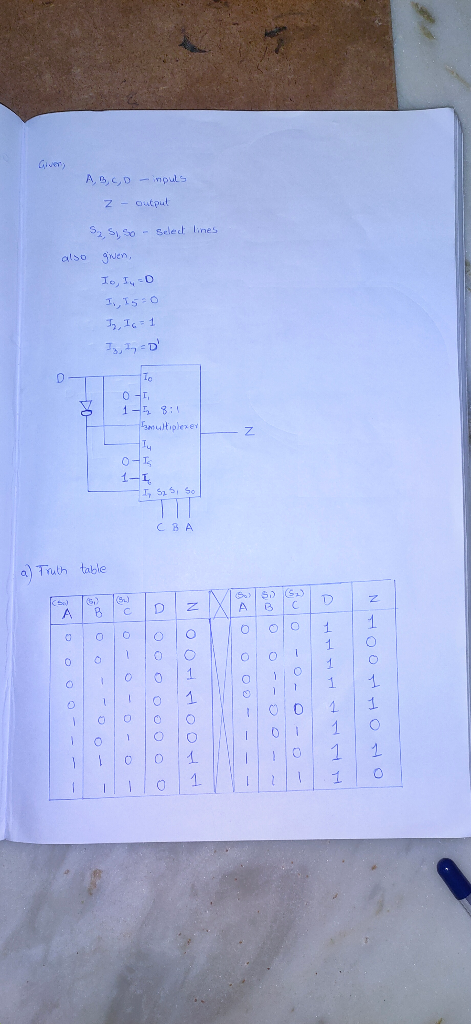
Given the following Karnaugh map AB CD 00 01 11 10 01 011 Draw a circuit...
 Given the following Karnaugh map AB CD 00 01 11 10 01 011 Draw a circuit that realizes the function above using one 8-to-1 multiplexer and any number of NAND gates. Observe that A, B and C are connected to the select inputs, SO, S1, and S2. 4-to-1 MUX -10 12 13 14 15 16 17 So Si S2 ABC
Please show step by step, complete solution and explain if possible. Thank you so much. 3....
 Please show step by step, complete solution and explain if
possible. Thank you so much.
3. Six-Sided Die Display Circuit In this problem, you will design a logic circuit to display the six faces of a die using 7 LEDs. For example, the value 5 is shown on the display below. Your circuit takes three bits XYZ as input and outputs the patterns shown in the table below, by lighting up the correspondind LEDs. For example, for the value 5,...
Please show step by step, complete solution and explain if
possible. Thank you so much.
3. Six-Sided Die Display Circuit In this problem, you will design a logic circuit to display the six faces of a die using 7 LEDs. For example, the value 5 is shown on the display below. Your circuit takes three bits XYZ as input and outputs the patterns shown in the table below, by lighting up the correspondind LEDs. For example, for the value 5,...
Please answer every part 1) Six Transistor CMOS Logic Circuit, Z-output; A, B, C are the...
 Please answer every part
1) Six Transistor CMOS Logic Circuit, Z-output; A, B, C are the inputs. 15 pts The three P-devices are connected as follows: Q2S-5V; Q2D-Q4S Q6S; Q4D-Q6D-Z. The three N-devices are connected as follows: QiS-GND Q3D-Q5S Q3S GNDQID-Q5D-Z The three inputs are connected as follows: A-QIG-Q2G; B-Q3G-Q4G; C Q5G Q6G. a) Draw the CMOS circuit. 3 pts b) Draw the function table for the three inputs, the six transistors and the output, Ζ. Use 0 for an...
Please answer every part
1) Six Transistor CMOS Logic Circuit, Z-output; A, B, C are the inputs. 15 pts The three P-devices are connected as follows: Q2S-5V; Q2D-Q4S Q6S; Q4D-Q6D-Z. The three N-devices are connected as follows: QiS-GND Q3D-Q5S Q3S GNDQID-Q5D-Z The three inputs are connected as follows: A-QIG-Q2G; B-Q3G-Q4G; C Q5G Q6G. a) Draw the CMOS circuit. 3 pts b) Draw the function table for the three inputs, the six transistors and the output, Ζ. Use 0 for an...
Please answer every part 1) Six Transistor CMOS Logic Circuit, Z-output; A, B, C are the inputs. 15 pts The three P-devices are connected as follows: Q2S-5V; Q2D-Q4S Q6S; Q4D-Q6D-Z. The three N-devic...
 Please answer every part
1) Six Transistor CMOS Logic Circuit, Z-output; A, B, C are the inputs. 15 pts The three P-devices are connected as follows: Q2S-5V; Q2D-Q4S Q6S; Q4D-Q6D-Z. The three N-devices are connected as follows: QiS-GND Q3D-Q5S Q3S GNDQID-Q5D-Z The three inputs are connected as follows: A-QIG-Q2G; B-Q3G-Q4G; C Q5G Q6G. a) Draw the CMOS circuit. 3 pts b) Draw the function table for the three inputs, the six transistors and the output, Ζ. Use 0 for an...
Please answer every part
1) Six Transistor CMOS Logic Circuit, Z-output; A, B, C are the inputs. 15 pts The three P-devices are connected as follows: Q2S-5V; Q2D-Q4S Q6S; Q4D-Q6D-Z. The three N-devices are connected as follows: QiS-GND Q3D-Q5S Q3S GNDQID-Q5D-Z The three inputs are connected as follows: A-QIG-Q2G; B-Q3G-Q4G; C Q5G Q6G. a) Draw the CMOS circuit. 3 pts b) Draw the function table for the three inputs, the six transistors and the output, Ζ. Use 0 for an...
EE 210 Digital Logic Experiment 3 - Basic Combinational Logic: Adjacency Tester- Simulation only. In this...
 EE 210 Digital Logic Experiment 3 - Basic Combinational Logic: Adjacency Tester- Simulation only. In this experiment, the student will design and simulate a minimal AND, OR and INVERTER circuit, with 4 input variables A, B, C, and D, and output F, that will produce a logic 1 output whenever two adjacent input variables are 1s. In this context, the A and D variables are also treated as being adjacent variables. See the partially filled-in Truth Table below, for more...
Objective: Practice converting a Boolean logic expression into it’s truth table and to show the implementation...
Objective: Practice converting a Boolean logic expression into it’s truth table and to show the implementation of the logic function with hardware logic gates. _ _ Given the Boolean logic expression for output D: A B C + A B C = D In the space below show how you would implement a circuit where the inputs are A, B and C and the output is D with standard logic gates. In the space below assemble the Truth...
 Show all steps of your solutions. Attach screen shots of your Logisim Solutions. Solutions without clear solution steps will be subject to maximum penalty I. Assume that A 100 in hexadecimal and B = 25 in octal. Perform the indicated operations: a. A - B using 2's comp b. B- A using 10's comp 2. Write Institute of Electrical and Electronics Engineers (IEEE) floating point (32 bit) representation of the decimal number -100. 625 lement method lement method 3. Design...
 Please solve ASAP
Problem #2 (100pts) Consider the circuit shown in the Logic Circuit in the Figure: Find its Truth Table 2) Use the SoP (Sum of Products) Karnaugh Map to identify an expression for X as a function of the inputs A, B and C
Problem #2 (100pts) Consider the circuit shown in the Logic Circuit in the Figure: Find its Truth Table 2) Use the SoP (Sum of Products) Karnaugh Map to identify an expression for X as...
Please solve ASAP
Problem #2 (100pts) Consider the circuit shown in the Logic Circuit in the Figure: Find its Truth Table 2) Use the SoP (Sum of Products) Karnaugh Map to identify an expression for X as a function of the inputs A, B and C
Problem #2 (100pts) Consider the circuit shown in the Logic Circuit in the Figure: Find its Truth Table 2) Use the SoP (Sum of Products) Karnaugh Map to identify an expression for X as...
 Problem 1:
consider the following circuit with 4 inputs A, B, c, D, and 3 outputs F, G, H. Each input/output is connected to an input/output port. 3-input OR gate Figure 1 a) Determine the Boolean algebra equations relating each input to each output of the circuit. b) Create the truth tables corresponding to the equations obtained above. There should be one truth table per equation c) Produce the Karnaugh maps corresponding to the truth tables d) Determine simplified Boolean...
Problem 1:
consider the following circuit with 4 inputs A, B, c, D, and 3 outputs F, G, H. Each input/output is connected to an input/output port. 3-input OR gate Figure 1 a) Determine the Boolean algebra equations relating each input to each output of the circuit. b) Create the truth tables corresponding to the equations obtained above. There should be one truth table per equation c) Produce the Karnaugh maps corresponding to the truth tables d) Determine simplified Boolean...
 Digital Logic Fundamentals. Need help with this
assignment!!!
Want to make sure I'm on the right track with the truth table
and K-MAPS.
Also I'd like to know how to design the LOGISIM circuit.
Thank you.
igital Logic Fundamentals An Excess-3 code exists for the following reason: The primary advantage of excess-3 coding over non-biased coding is that a decimal number can be nines' complemented (for subtraction) as easily as a binary number can be ones' complemented: just by inverting...
Digital Logic Fundamentals. Need help with this
assignment!!!
Want to make sure I'm on the right track with the truth table
and K-MAPS.
Also I'd like to know how to design the LOGISIM circuit.
Thank you.
igital Logic Fundamentals An Excess-3 code exists for the following reason: The primary advantage of excess-3 coding over non-biased coding is that a decimal number can be nines' complemented (for subtraction) as easily as a binary number can be ones' complemented: just by inverting...
 Given the following Karnaugh map AB CD 00 01 11 10 01 011 Draw a circuit that realizes the function above using one 8-to-1 multiplexer and any number of NAND gates. Observe that A, B and C are connected to the select inputs, SO, S1, and S2. 4-to-1 MUX -10 12 13 14 15 16 17 So Si S2 ABC
 Please show step by step, complete solution and explain if
possible. Thank you so much.
3. Six-Sided Die Display Circuit In this problem, you will design a logic circuit to display the six faces of a die using 7 LEDs. For example, the value 5 is shown on the display below. Your circuit takes three bits XYZ as input and outputs the patterns shown in the table below, by lighting up the correspondind LEDs. For example, for the value 5,...
Please show step by step, complete solution and explain if
possible. Thank you so much.
3. Six-Sided Die Display Circuit In this problem, you will design a logic circuit to display the six faces of a die using 7 LEDs. For example, the value 5 is shown on the display below. Your circuit takes three bits XYZ as input and outputs the patterns shown in the table below, by lighting up the correspondind LEDs. For example, for the value 5,...
 Please answer every part
1) Six Transistor CMOS Logic Circuit, Z-output; A, B, C are the inputs. 15 pts The three P-devices are connected as follows: Q2S-5V; Q2D-Q4S Q6S; Q4D-Q6D-Z. The three N-devices are connected as follows: QiS-GND Q3D-Q5S Q3S GNDQID-Q5D-Z The three inputs are connected as follows: A-QIG-Q2G; B-Q3G-Q4G; C Q5G Q6G. a) Draw the CMOS circuit. 3 pts b) Draw the function table for the three inputs, the six transistors and the output, Ζ. Use 0 for an...
Please answer every part
1) Six Transistor CMOS Logic Circuit, Z-output; A, B, C are the inputs. 15 pts The three P-devices are connected as follows: Q2S-5V; Q2D-Q4S Q6S; Q4D-Q6D-Z. The three N-devices are connected as follows: QiS-GND Q3D-Q5S Q3S GNDQID-Q5D-Z The three inputs are connected as follows: A-QIG-Q2G; B-Q3G-Q4G; C Q5G Q6G. a) Draw the CMOS circuit. 3 pts b) Draw the function table for the three inputs, the six transistors and the output, Ζ. Use 0 for an...
 EE 210 Digital Logic Experiment 3 - Basic Combinational Logic: Adjacency Tester- Simulation only. In this experiment, the student will design and simulate a minimal AND, OR and INVERTER circuit, with 4 input variables A, B, C, and D, and output F, that will produce a logic 1 output whenever two adjacent input variables are 1s. In this context, the A and D variables are also treated as being adjacent variables. See the partially filled-in Truth Table below, for more...
Most questions answered within 3 hours.
-
Write a program to score the paper-rock-scissor game. Each of
two users types in either P,R...
asked 3 minutes ago -
Calculate the equillibrium constent K for a redox reaction that
has E°cell = -.98 V at...
asked 15 minutes ago -
A concave spherical mirror has a radius of curvature of
magnitude 19.6 cm.
(a) Find the...
asked 17 minutes ago -
3. draw a diagram of the magnetic field:
a. around a long straight wire with a...
asked 16 minutes ago -
If you titrated 30.0 mL of 0.1 M HCl with 0.1 M NaOH, indicate
the approximate...
asked 24 minutes ago -
NADH passes electrons into the electron transport chain. List
the carriers that would receive the electrons,...
asked 32 minutes ago -
A cylindrical cable with a resistivity of 1.6x10⁻⁸ Ω·m and cross
sectional area of 3x10⁻⁵ m^2...
asked 32 minutes ago -
True or False.
A consumer with convex preferences who is indifferent between
the bundles (5,2) and...
asked 36 minutes ago -
A diamond's index of refraction for red light, 656 nm, is 2.410,
while that for blue...
asked 49 minutes ago -
Compare HPLC, SPE, and GC. Identify the differences, the
advantages, and the weaknesses of each method.
asked 50 minutes ago -
Characteristic x-rays emitted by potassium have a wavelength of
0.374 nm. What is the energy of...
asked 52 minutes ago -
there is a function to create two random numbers between 1 and
25 and a function...
asked 1 hour ago