
Homework Answers


Add Answer to:
1. (a) Draw the band diagram for phosphorous doped silicon, including both the majority and minority...
3. Silicon samples with band-gas 1.1 eV at 300 Kelvin, are doped at four different levels...
 3. Silicon samples with band-gas 1.1 eV at 300 Kelvin, are doped at four different levels and have the properties listed below. Case 1: Case 2: Case 3: Case 4: Ex-Ey = 0.15 eV Ef-Ey=0.88 eV EF-Ey = 0.55 eV Ex-Ey = 1.09 eV The four cases above show the position of the Fermi Level Er relative to the valence band edge Ev.at dilterent doping levels. a) identify each sample as degenerate and nondegenerate. b) which nondegenerate case shows heavy...
5. (20 points) A Silicon sample contains a small amount (1018 atoms/cm) of phosphorous (P) impurity....
 5. (20 points) A Silicon sample contains a small amount (1018 atoms/cm) of phosphorous (P) impurity. (a) What is the majority charge carrier at room temperature? (b) Calculate the resistivity of this material at room temperature. Please show any assumption used in calculation. The mobility of this charge carrier is 700 cm /Vs at room temperature. (e) Show schematically the temperature effects on the mobility, concentration and conductivity of this semiconductor. 6. (20 points) For Mºsc, show schematically (a) the...
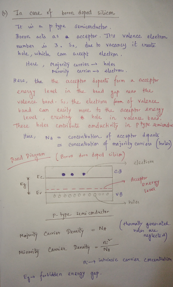
Draw and label (valence and conduction) a band diagram for an extrinsic semiconductor with silicon as...
 Draw and label (valence and conduction) a band diagram for an extrinsic semiconductor with silicon as the substrate and indium as the dopant. (Please make it as least 1/3 of a page in size.) Write down on the page whether it is an n-type or a p-type. 1 i. - BIO E % Explain briefly how you would adjust the semiconductor in the previous question if you wanted to allow a higher limiting current to pass through. (type your answer...
1. Draw the schematics of forward-biased and negative-biased diodes. Show the polarity of voltage source (positive...
1. Draw the schematics of forward-biased and negative-biased diodes. Show the polarity of voltage source (positive and negative terminal of the source), the position of Fermi levels and the current direction. Explain why there is a small current flow when a p-n junction is under reverse bias. 2. A p-n junction can be made by diffusing acceptor atoms into an n-type semiconductor. Suppose that boron is diffused into a silicon wafer doped with arsenic at 1015 cm-3 such that the...
1. What is a dopant and how is it used in modern semiconductors 2. What is...
 1. What is a dopant and how is it used in modern semiconductors 2. What is the difference total ionization and dielectric breakdown, at what temperature can we assume total ionization has occurred? 3. Write the Thermal Voltage Vr kT for the following temperatures: a. T 300K, Vr b.T 600K, Vr c. T 750K, Vr d. T 1200K, Vr e. T 150K, Vr 4. Draw the Density of States (DOS) as a function of Energy for a semiconductor, label the...
A3. (a) Draw a band diagram and a cross-sectional diagram of an abrupt p-n junction0Marks] with N...
 a3. (a) Draw a band diagram and a cross-sectional diagram of an abrupt p-n junction0Marks] with N>N at thermal equilibrium at 300K and label the following: () Diffusion currents, (i) Drift currents (ii) Fermi level, (iv) SCR, (v) QNR, (vi) Contact potential with polarity, (vi) Electric field distribution in the SCR, (vii) Electrostatic potential distribution in SCR, (ix) SCR charges, and (x) SCR penetration into the p-and n sides. (b) In a p'-n junction at 300K, the n side has...
Taking pure silicon (Si) as an example, explain what is meant by the terms electron-hole generation...
 Taking pure silicon (Si) as an example, explain what is meant by the terms electron-hole generation and recombination, how they affect the electrical conductivity, and define what is meant by the "intrinsic carrier density", n. [5 marks] Q3. a) b) With the aid of both lattice and energy band diagrams, explain how n-type doping of Si is achieved and state two types of suitable dopant atoms. [7 marks] c) An n-type region on a Si wafer has a donor concentration...
EENG 245 Physical electronics HW 1 1) The NaCl crystal is cubic, and can be described...
 EENG 245 Physical electronics HW 1 1) The NaCl crystal is cubic, and can be described as follows. Na atoms sit at the corners and faces of a cube, and Cl atoms sit in between two Na atoms. This means that a Clatom is found half-way along each of the cube edges, and there is a Cl in the center of the cube. (We could also have described the lattice by interchanging Na and Cl in the description above.) Another...
Solve question 3 Only, Be very clear/ about evry single step Mark all currents/ voltages assign...
 Solve question 3 Only, Be very clear/ about evry single
step
Mark all currents/ voltages
assign label and polarity
redraw simplified circuits
then write KVL and KCl equations dont use values, write plain
equations first then apply Ohms law.
Substitute values last. in equations
solve equations for unknowns show step by step solution for
each unknown.
write clearly. evry step.
Do In Every Circuit app
Do only question 3 and attach screenshot of the outputs.
Make sure answers found match...
Solve question 3 Only, Be very clear/ about evry single
step
Mark all currents/ voltages
assign label and polarity
redraw simplified circuits
then write KVL and KCl equations dont use values, write plain
equations first then apply Ohms law.
Substitute values last. in equations
solve equations for unknowns show step by step solution for
each unknown.
write clearly. evry step.
Do In Every Circuit app
Do only question 3 and attach screenshot of the outputs.
Make sure answers found match...
Database 1. Draw an Entity-Relationship diagram(including cardinality ratio and participa- tion constraint) to represent the following...
 Database
1. Draw an Entity-Relationship diagram(including cardinality ratio and participa- tion constraint) to represent the following application: A DEPARTMENT has a number of TEACHERS and each TEACHER is affil- iated only with one DEPARTMENT; A STUDENT has only one TEACHER as an advisor, but a TEACHER can advise many STUDENT; on the other hand, TEACHER instructs many STUDENTS, and a STUDENT has a number of instructors. Different AGENCIES support different TEACHERS for various PROJECTS. (15 points) A trucking company is...
Database
1. Draw an Entity-Relationship diagram(including cardinality ratio and participa- tion constraint) to represent the following application: A DEPARTMENT has a number of TEACHERS and each TEACHER is affil- iated only with one DEPARTMENT; A STUDENT has only one TEACHER as an advisor, but a TEACHER can advise many STUDENT; on the other hand, TEACHER instructs many STUDENTS, and a STUDENT has a number of instructors. Different AGENCIES support different TEACHERS for various PROJECTS. (15 points) A trucking company is...
 3. Silicon samples with band-gas 1.1 eV at 300 Kelvin, are doped at four different levels and have the properties listed below. Case 1: Case 2: Case 3: Case 4: Ex-Ey = 0.15 eV Ef-Ey=0.88 eV EF-Ey = 0.55 eV Ex-Ey = 1.09 eV The four cases above show the position of the Fermi Level Er relative to the valence band edge Ev.at dilterent doping levels. a) identify each sample as degenerate and nondegenerate. b) which nondegenerate case shows heavy...
 5. (20 points) A Silicon sample contains a small amount (1018 atoms/cm) of phosphorous (P) impurity. (a) What is the majority charge carrier at room temperature? (b) Calculate the resistivity of this material at room temperature. Please show any assumption used in calculation. The mobility of this charge carrier is 700 cm /Vs at room temperature. (e) Show schematically the temperature effects on the mobility, concentration and conductivity of this semiconductor. 6. (20 points) For Mºsc, show schematically (a) the...
 Draw and label (valence and conduction) a band diagram for an extrinsic semiconductor with silicon as the substrate and indium as the dopant. (Please make it as least 1/3 of a page in size.) Write down on the page whether it is an n-type or a p-type. 1 i. - BIO E % Explain briefly how you would adjust the semiconductor in the previous question if you wanted to allow a higher limiting current to pass through. (type your answer...
 1. What is a dopant and how is it used in modern semiconductors 2. What is the difference total ionization and dielectric breakdown, at what temperature can we assume total ionization has occurred? 3. Write the Thermal Voltage Vr kT for the following temperatures: a. T 300K, Vr b.T 600K, Vr c. T 750K, Vr d. T 1200K, Vr e. T 150K, Vr 4. Draw the Density of States (DOS) as a function of Energy for a semiconductor, label the...
 a3. (a) Draw a band diagram and a cross-sectional diagram of an abrupt p-n junction0Marks] with N>N at thermal equilibrium at 300K and label the following: () Diffusion currents, (i) Drift currents (ii) Fermi level, (iv) SCR, (v) QNR, (vi) Contact potential with polarity, (vi) Electric field distribution in the SCR, (vii) Electrostatic potential distribution in SCR, (ix) SCR charges, and (x) SCR penetration into the p-and n sides. (b) In a p'-n junction at 300K, the n side has...
 Taking pure silicon (Si) as an example, explain what is meant by the terms electron-hole generation and recombination, how they affect the electrical conductivity, and define what is meant by the "intrinsic carrier density", n. [5 marks] Q3. a) b) With the aid of both lattice and energy band diagrams, explain how n-type doping of Si is achieved and state two types of suitable dopant atoms. [7 marks] c) An n-type region on a Si wafer has a donor concentration...
 EENG 245 Physical electronics HW 1 1) The NaCl crystal is cubic, and can be described as follows. Na atoms sit at the corners and faces of a cube, and Cl atoms sit in between two Na atoms. This means that a Clatom is found half-way along each of the cube edges, and there is a Cl in the center of the cube. (We could also have described the lattice by interchanging Na and Cl in the description above.) Another...
 Solve question 3 Only, Be very clear/ about evry single
step
Mark all currents/ voltages
assign label and polarity
redraw simplified circuits
then write KVL and KCl equations dont use values, write plain
equations first then apply Ohms law.
Substitute values last. in equations
solve equations for unknowns show step by step solution for
each unknown.
write clearly. evry step.
Do In Every Circuit app
Do only question 3 and attach screenshot of the outputs.
Make sure answers found match...
Solve question 3 Only, Be very clear/ about evry single
step
Mark all currents/ voltages
assign label and polarity
redraw simplified circuits
then write KVL and KCl equations dont use values, write plain
equations first then apply Ohms law.
Substitute values last. in equations
solve equations for unknowns show step by step solution for
each unknown.
write clearly. evry step.
Do In Every Circuit app
Do only question 3 and attach screenshot of the outputs.
Make sure answers found match...
 Database
1. Draw an Entity-Relationship diagram(including cardinality ratio and participa- tion constraint) to represent the following application: A DEPARTMENT has a number of TEACHERS and each TEACHER is affil- iated only with one DEPARTMENT; A STUDENT has only one TEACHER as an advisor, but a TEACHER can advise many STUDENT; on the other hand, TEACHER instructs many STUDENTS, and a STUDENT has a number of instructors. Different AGENCIES support different TEACHERS for various PROJECTS. (15 points) A trucking company is...
Database
1. Draw an Entity-Relationship diagram(including cardinality ratio and participa- tion constraint) to represent the following application: A DEPARTMENT has a number of TEACHERS and each TEACHER is affil- iated only with one DEPARTMENT; A STUDENT has only one TEACHER as an advisor, but a TEACHER can advise many STUDENT; on the other hand, TEACHER instructs many STUDENTS, and a STUDENT has a number of instructors. Different AGENCIES support different TEACHERS for various PROJECTS. (15 points) A trucking company is...
Most questions answered within 3 hours.
-
Question Three
Suppose you as project manager are using the Waterfall
development methodology on a large...
asked 3 minutes ago -
Which statement is not true about welfare in Canada?
A.Benefits typically vary based on one's ability...
asked 35 minutes ago -
Please help me with FLOWCHART and UML diagram for class,
thank you!
#include <iostream>
#include <fstream>...
asked 1 hour ago -
3. Describe the “logic circuit” of the Lac operon. Which
proteins are bound or not to...
asked 1 hour ago -
Ayesha’s adjusted gross income is $60,000 in 2019. She donated a
piece of artwork with a...
asked 1 hour ago -
For Dijkstra’s shortest path algorithm:
a. Give the Big-O time for Dijkstra’s shortest path algorithm
and...
asked 1 hour ago -
Phosphorus violates the 'octet rule' in biological molecules,
forming more covalent bonds than expected based on...
asked 1 hour ago -
A 1.3 eV electron has a 10-4 probability of tunneling
through a 2.4 eV potential barrier....
asked 2 hours ago -
What is the one ingredient that is common to being successful
with all stakeholders?
profit
trust...
asked 2 hours ago -
Write an assembly language 32 bit program that reads in lines of
text by a .txt...
asked 2 hours ago -
what is the density ( in g/L) of hydrogen gas at 29 degrees C and a...
asked 2 hours ago -
5-6. You are considering three investment alternatives for some
spare cash: Old Reliable Corporation stock (A1),...
asked 2 hours ago