Draw the high and low freq C-V relation for an p-channel(n substrate) MOS capacitor and show...
Draw the high and low freq C-V relation for an p-channel(n
substrate) MOS capacitor and show important capacitance
and show important values & regimes Explain what values
mean.
Homework Answers
Metal Oxide Semiconductor (MOS) Capacitor
The MOS capacitor structure is shown in Figure 1. The “metal” plate
is a heavily doped p+
-
poly-silicon layer which behaves as a metal. The insulating layer
is silicon dioxide and the other
plate of the capacitor is the semiconductor layer which in our case
is n-type silicon whose
resistivity is 1-10 Ω-cm corresponding to a doping of 1015
cm-3.
The capacitance of the MOS structure depends on the voltage (bias)
on the gate. For the purposes
of this discussion, we shall refer to the contact to the
semiconductor as the body (B) while the
poly-silicon is called the gate (G). Typically a voltage is applied
to the gate while the body is
grounded and the applied voltage is VG but more accurately VGB. The
two (VG & VGB) will be
used interchangeably in this document. 
The capacitance depends on the voltage that is applied to the
gate (with respect to the body). The
dependence is shown in Figure 2 and there are roughly three regimes
of operation separated by
two voltages. The regimes are described by what is happening to the
semiconductor surface.
These are (1) Accumulation in which carriers of the same type as
the body accumulates at the
surface (2) Depletion in which the surface is devoid of any
carriers leaving only a space charge
or depletion layer, and (3) Inversion in which carriers of the
opposite type from the body
aggregate at the surface to “invert” the conductivity type. The two
voltages that demarcate the
three regimes are (a) Flatband Voltage (VFB) which separates the
accumulation regime from the
depletion regimes and (b) the Threshold Voltage (VT) which
demarcates the depletion regime
from the inversion regime
. 
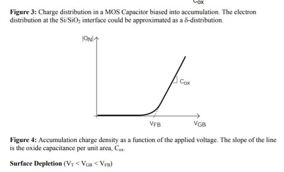
Figure 2: Capacitance per unit area vs. Gate Voltage (CV)
diagram of a MOS Capacitor. The
flatband voltage (VFB) separates the Accumulation region from the
Depletion regime. The
threshold voltage (VT) separates the depletion regime from the
inversion regime. CHF is high
frequency capacitance while CQS is quasi-static or low frequency
capacitance.
Surface Accumulation (VGB > VFB)
An applied positive gate voltage larger than the flatband voltage
(which will be defined shortly)
(VGB > VFB) induces positive charge on the “metal” gate and
negative charge in the
semiconductor. The only negative charges available are electrons
and they accumulate at the
surface. The electron concentration at the surface is above the
bulk value, thus leading to a
condition that is called surface accumulation. The charge
distribution and equivalent circuit is
shown in Figure 3. The flatband voltage (VFB) is the voltage at
which there is no charge on the
plates of the capacitor and hence there is no electric field across
the oxide. It’s numerical value
depends on the doping of the semiconductor and on any residual
interface charge that may exist
at the interface between the semiconductor and the insulator. When
the surface of the
semiconductor is accumulated, a plot of the charge per unit area
(QN) at the semiconductor /
oxide interface versus the applied voltage (VGB) is linear and the
slope is the oxide capacitance
per unit area., Cox., which is given by
ox
ox
MOS accumulation ox t
C C C ε , = max = =
where εox is the permittivity of the oxide and it is 3.9εo. εo is
the permittivity of free space or air.
εo = 8.854x10⁻¹⁴
Fcm-1. The unit for Cox is Fcm-2. Figure 4 is a plot of the charge
per unit area
(QN) as a function of the applied voltage (VGB). 
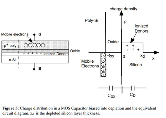
Surface Depletion (VT < VGB < VFB)
If the applied gate voltage is brought below the flat band voltage
(remember the flat band voltage
is the gate voltage at which there is no charge in the MOS
capacitor), a negative charge is
induced at the interface between the poly-silicon gate and the
oxide. This leads to a positive
charge being induced at the other interface i.e. the oxide /
semiconductor interface. This could
only be accomplished by “pushing” all the mobile negative carriers
(electrons) away and
exposing the fixed positive charge from the donors. Hence the
surface of the semiconductor is
depleted of mobile carriers leaving behind a positive space charge.
Figure 5 shows the charge
distribution under these circumstances. The space charge layer
resulting behaves also like a
capacitor having a capacitance per unit area (CD), which depends on
VGB and is given by 
Add Answer to:
Draw the high and low freq C-V relation for an p-channel(n
substrate) MOS capacitor and show...
Derive C-V characteristics for n-type MOS at high frequency and low frequency (10points). Hints: Strong inversion...
 Derive C-V characteristics for n-type MOS at high frequency and
low frequency (10points).
Hints:
Strong inversion Accumulation Depletion Moderate inversion Figure 10.271 Ideal low-frequency capacitance versus gate voltage of a MOS capacitor with an n-type substrate.
Derive C-V characteristics for n-type MOS at high frequency and
low frequency (10points).
Hints:
Strong inversion Accumulation Depletion Moderate inversion Figure 10.271 Ideal low-frequency capacitance versus gate voltage of a MOS capacitor with an n-type substrate.
Problem 1. An n-channel MOS transistor is fabricated with the following specifications: Substrate is a p-type...
Problem 1. An n-channel MOS transistor is fabricated with the following specifications: Substrate is a p-type silicon with doping concentration NA=2x1015 cm-3 . The SiO2 gate thickness is 200 Å. Effective interface charges Qi=6.5x10⁻⁹ col/cm2. Work function difference between gate conductor and silicon substrate qфms=-0.95 eV. Calculate the following: a. Maximum depletion width, with respect to ground b. Gate capacitance per unit area, Ci c. Flat-band voltage, VFB d. Threshold voltage, VT.
(3 pts) 8. Consider an n-channel MOSFET, which is essentially a MOS capacitor with two p-n...
 (3 pts) 8. Consider an n-channel MOSFET, which is essentially a MOS capacitor with two p-n junctions placed immediately adjacent to the region of the semiconductor controlled by the MOS gate. What must be the biasing mode of the MOS structure and polarity of the gate voltage for there to be a measurable current? a. Enhancement, positive b. Inversion, negative c. Inversion, positive d. Depletion, negative
Problem 5: The gate capacitance vs. gate voltage characteristic of a p+ poly-Si gated MOS capacitor of area 1x10"cm', is as shown: Assume Esi = 11.9, Eox-39,E,-8.85 × 10⁻¹⁴ F/on, and nl =...
 Problem 5: The gate capacitance vs. gate voltage characteristic of a p+ poly-Si gated MOS capacitor of area 1x10"cm', is as shown: Assume Esi = 11.9, Eox-39,E,-8.85 × 10⁻¹⁴ F/on, and nl = 1.5 x 1010 cm3 Co [Farads] 3.45x10¹¹ >Va [Volts] 1.0 0.3 (a) Is the semiconductor (silicon) substrate doped n-type or p-type? Explain briefly. (b) Is the measurement frequency low or high? Explain briefly. (c) What is the thickness of the gate oxide (SiO2), xo? (d) Estimate the...
Section B (total 60 marks for section B) B1 a) An MOS capacitor has a p-type semiconductor substrate doped with an impu...
 Section B (total 60 marks for section B) B1 a) An MOS capacitor has a p-type semiconductor substrate doped with an impurity concentration of 1018 cm3. Assume a poly-Si material is used for the gate. Draw a diagram of the capacitor structure showing material types and an energy band diagram it is in thermal equilibrium. (10 marks) b) Given an MOS capacitor with a p-type semiconductor substrate and poly-Si material as gate (in part a), what is the meaning of...
6. A MOS system has an n+ polysilicon gate and a p-type silicon substrate doped to...
 6. A MOS system has an n+ polysilicon gate and a p-type silicon substrate doped to N. =10cm. Assume there is an oxide surface charge density (Q,/q) = 100cm 2. Design the oxide thickness so that V1 = 0.5 V (no bias is applied between the channel and substrate). Answer: x 58.5 nm OX
1.24P)a) Plot the structure of p-channel MOS-FET (Show semiconductor structure, gate, drain, source and voltage polarities)...
 1.24P)a) Plot the structure of p-channel MOS-FET (Show semiconductor structure, gate, drain, source and voltage polarities) and summarize the working principle. b) Explain what happens if you change drain source voltage polarity. c) Plot the band diagram, approximate distributions of charge, electric field, and electrostatic potential in the ideal MOS capacitor in inversion for the p-channel case.
Problem 6: oxide charge in MOS capacitance Consider the C-V curve of a MOS capacitor in...
 Problem 6: oxide charge in MOS capacitance Consider the C-V curve of a MOS capacitor in the figure (the solid line). The capacitor area is 6400 m Co-45 pF and C,-5.6pF Cox C1 V. Av If, due to the oxide fixed charge, the C-V curve shifted from the solid line to the dashed line with ΔⅤ 0.05V, what is the charge polarity and the area density (C/em2) of the oxide fixed charge?
Q2. a) Draw the cross-sectional view of ann channel MOS transistor. Label the necessary parts (L,...
 Q2. a) Draw the cross-sectional view of ann channel MOS transistor. Label the necessary parts (L, W, toi, D,G,S, etc.) Give appropriate values for L, W, tox. (10 p) b) Explain, how an n-channel enhancement mode MOS transistor operates. (10p)
 Derive C-V characteristics for n-type MOS at high frequency and
low frequency (10points).
Hints:
Strong inversion Accumulation Depletion Moderate inversion Figure 10.271 Ideal low-frequency capacitance versus gate voltage of a MOS capacitor with an n-type substrate.
Derive C-V characteristics for n-type MOS at high frequency and
low frequency (10points).
Hints:
Strong inversion Accumulation Depletion Moderate inversion Figure 10.271 Ideal low-frequency capacitance versus gate voltage of a MOS capacitor with an n-type substrate.
 (3 pts) 8. Consider an n-channel MOSFET, which is essentially a MOS capacitor with two p-n junctions placed immediately adjacent to the region of the semiconductor controlled by the MOS gate. What must be the biasing mode of the MOS structure and polarity of the gate voltage for there to be a measurable current? a. Enhancement, positive b. Inversion, negative c. Inversion, positive d. Depletion, negative
 Problem 5: The gate capacitance vs. gate voltage characteristic of a p+ poly-Si gated MOS capacitor of area 1x10"cm', is as shown: Assume Esi = 11.9, Eox-39,E,-8.85 × 10⁻¹⁴ F/on, and nl = 1.5 x 1010 cm3 Co [Farads] 3.45x10¹¹ >Va [Volts] 1.0 0.3 (a) Is the semiconductor (silicon) substrate doped n-type or p-type? Explain briefly. (b) Is the measurement frequency low or high? Explain briefly. (c) What is the thickness of the gate oxide (SiO2), xo? (d) Estimate the...
 Section B (total 60 marks for section B) B1 a) An MOS capacitor has a p-type semiconductor substrate doped with an impurity concentration of 1018 cm3. Assume a poly-Si material is used for the gate. Draw a diagram of the capacitor structure showing material types and an energy band diagram it is in thermal equilibrium. (10 marks) b) Given an MOS capacitor with a p-type semiconductor substrate and poly-Si material as gate (in part a), what is the meaning of...
 6. A MOS system has an n+ polysilicon gate and a p-type silicon substrate doped to N. =10cm. Assume there is an oxide surface charge density (Q,/q) = 100cm 2. Design the oxide thickness so that V1 = 0.5 V (no bias is applied between the channel and substrate). Answer: x 58.5 nm OX
 1.24P)a) Plot the structure of p-channel MOS-FET (Show semiconductor structure, gate, drain, source and voltage polarities) and summarize the working principle. b) Explain what happens if you change drain source voltage polarity. c) Plot the band diagram, approximate distributions of charge, electric field, and electrostatic potential in the ideal MOS capacitor in inversion for the p-channel case.
 1.24P)a) Plot the structure of p-channel MOS-FET (Show semiconductor structure, gate, drain, source and voltage polarities) and summarize the working principle. b) Explain what happens if you change drain source voltage polarity. c) Plot the band diagram, approximate distributions of charge, electric field, and electrostatic potential in the ideal MOS capacitor in inversion for the p-channel case.
 Problem 6: oxide charge in MOS capacitance Consider the C-V curve of a MOS capacitor in the figure (the solid line). The capacitor area is 6400 m Co-45 pF and C,-5.6pF Cox C1 V. Av If, due to the oxide fixed charge, the C-V curve shifted from the solid line to the dashed line with ΔⅤ 0.05V, what is the charge polarity and the area density (C/em2) of the oxide fixed charge?
 Q2. a) Draw the cross-sectional view of ann channel MOS transistor. Label the necessary parts (L, W, toi, D,G,S, etc.) Give appropriate values for L, W, tox. (10 p) b) Explain, how an n-channel enhancement mode MOS transistor operates. (10p)
Most questions answered within 3 hours.
-
You purchase your daily coffee at the Chemist’s Coffeehouse and
have a choice of two cups:...
asked 1 hour ago -
Which of the following pairs of chemicals could be used to make
a buffer solution?
A.)...
asked 1 hour ago -
Problem 16-51 Sales
Activity Variance (LO 16-3)Odessa, Inc., reports the following
information concerning operations for the...
asked 2 hours ago -
Pictured on the right are thee point charges Q1 = 18.4 μC, Q2 =
-30.6 μC,...
asked 2 hours ago -
A graduate student is conducting research in psychology and
needs to obtain the IQ scores of...
asked 3 hours ago -
R2.84: There are 2 defective products in a production lot of 10.
An inspector randomly selected...
asked 4 hours ago -
Consider the following equilibrium system: COCl2(g) CO(g) +
Cl2(g) A 10.00 L evacuated flask is filled...
asked 4 hours ago -
1) What are the two distinct steps that one needs to perform
when developing a data...
asked 4 hours ago -
2) Write a C++ program that uses a class called “Degree” to
obtain the trigonometric
values...
asked 6 hours ago -
1. In eukaryotic cells the genomes of
&
asked 5 hours ago -
The standard enthalpy of propanol (C3H7OH) is -303.0 kJ/mol.
Compute both of the
gross and net...
asked 5 hours ago -
Why PWM using H-bridge for control motor speed is more power
effiecient than the linear amplifier...
asked 6 hours ago