
Homework Answers

Add Answer to:
6. A MOS system has an n+ polysilicon gate and a p-type silicon substrate doped to...
Consider an n-channel Silicon MOS system with a substrate resistivity of 10 0-cm and with a...
 Consider an n-channel Silicon MOS system with a substrate resistivity of 10 0-cm and with a polycrystalline gate. Assume that the polysilicon gate is doped with boron atoms to a density of 1x1019 cm and that the silicon dioxide is 50 nm-thick. The channel is not biased except from the gate (Vc= VB = 0). (i) Accurately sketch the band diagram identifying flatband voltage, surface potential at inversion, depletion width at inversion, and charges at inversion. Tabulate these parameters. (ii)...
A MOS capacitor is made on n-type silicon with oxide thickness of 50 A, a positive interface charge of 5 x 1010 cm2 and...
 A MOS capacitor is made on n-type silicon with oxide thickness of 50 A, a positive interface charge of 5 x 1010 cm2 and a uniform positive oxide charge of density p- 2 x 106 cm3 throughout the oxide. The substrate is doped with Na-101" cm3 and the gate is polysilicon doped with boron just to the edge of degeneracy (p+ poly, Ef -Ev). a. Calculate the flat band voltage VB and the threshold voltage Vr b. Sketch the charge...
1. MOSFET is made on silicon substrate doped with boron to a concentration of 5x1027 cm....
 1. MOSFET is made on silicon substrate doped with boron to a concentration of 5x1027 cm. Silicon oxide layer of thickness 5 nm is used as an insulator. Gate electrode is made of n-type polysilicon doped to a concentration of 8x1018 cm Width and length of the transistor are 10 micrometer and 100 nm respectively. For this transistor find: a) saturation drain voltage at gate voltage 7 V; b) transconductance at gate voltage 6 V. 160 mev 140
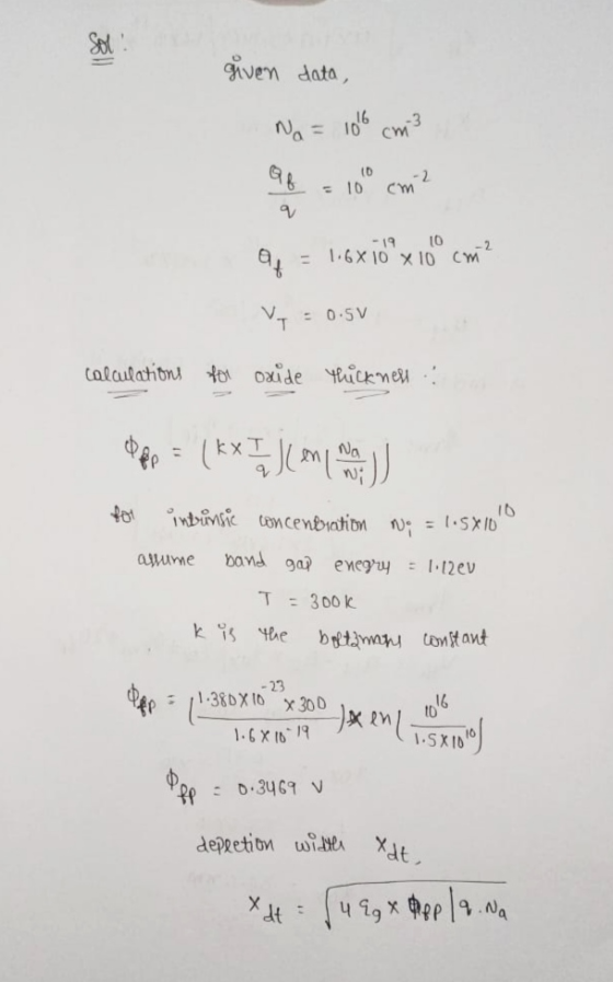
Problem 3 (25 points) Consider a MOS capacitor with p polysilicon gate and p-type silicon substrate with NA 1016 cm3. Ef- Ev in the polysilicon gate. Assume the following parameters: I200A, , 1.5x10°...
 Problem 3 (25 points) Consider a MOS capacitor with p polysilicon gate and p-type silicon substrate with NA 1016 cm3. Ef- Ev in the polysilicon gate. Assume the following parameters: I200A, , 1.5x10° cm*,E, -3.9x8.854x104FIcm ox a) (5 points) Calculate the metal-semiconductor work function difference. b) (5 points) Calculate the surface potential at the threshold inversion. c) (5 points) Calculate the depletion width (in μm) at the threshold inversion. d) (5 points) Calculate the flat band voltage. e) (5 points)...
3. A MOSFET is made on silicon substrate doped with boron with a concentration of 1018 cm. Width and length of channel are 100 and 0.1 micron respectively. Thickness of the oxide insulator under the...
 3. A MOSFET is made on silicon substrate doped with boron with a concentration of 1018 cm. Width and length of channel are 100 and 0.1 micron respectively. Thickness of the oxide insulator under the gate is 10 nm. Find transconductance of this transistor and saturation current at gate voltage 6 V. kT (Nc Si eNa2egp Cox
3. A MOSFET is made on silicon substrate doped with boron with a concentration of 1018 cm. Width and length of channel are...
3. A MOSFET is made on silicon substrate doped with boron with a concentration of 1018 cm. Width and length of channel are 100 and 0.1 micron respectively. Thickness of the oxide insulator under the gate is 10 nm. Find transconductance of this transistor and saturation current at gate voltage 6 V. kT (Nc Si eNa2egp Cox
3. A MOSFET is made on silicon substrate doped with boron with a concentration of 1018 cm. Width and length of channel are...
In the silicon-based n-channel MOSMET. the work function of gate electrode 4a 4.08eV and the elec...
 In the silicon-based n-channel MOSMET. the work function of gate electrode 4a 4.08eV and the electron affinity of silicon χ = 4.05eV. The fixed oxide charge located at Si-SiO2 interface has a density of 5x10¹⁴ m-2 . The silicon substrate is doped with boron atoms in a concentration of 2x10*°m3. The oxide layer has a thickness of 200nm. Calculate (i) the flat band voltage, (ii) the threshold voltage to induce the inversion layer and ii) the maximum, minimum and flat...
Please answer question with the formulas given 3. A MOSFET is made on silicon substrate doped with boron with a concentration of 10 cm2. Width and length of channel are 100 and 0.1 micron respect...
 Please answer question with the formulas given
3. A MOSFET is made on silicon substrate doped with boron with a concentration of 10 cm2. Width and length of channel are 100 and 0.1 micron respectively. Thickness of the oxide insulator under the gate is 10 nm. Find transconductance of this transistor and saturation current at gate voltage 6 V kT, (Nc In Na 2 KTN
3. A MOSFET is made on silicon substrate doped with boron with a concentration of...
Please answer question with the formulas given
3. A MOSFET is made on silicon substrate doped with boron with a concentration of 10 cm2. Width and length of channel are 100 and 0.1 micron respectively. Thickness of the oxide insulator under the gate is 10 nm. Find transconductance of this transistor and saturation current at gate voltage 6 V kT, (Nc In Na 2 KTN
3. A MOSFET is made on silicon substrate doped with boron with a concentration of...
For an ideal MOS structure, the SiO2 thickness is 150 A, and the substrate is doped...
 For an ideal MOS structure, the SiO2 thickness is 150 A, and the substrate is doped with 2x10¹⁶/ cm3 acceptors. Determine the threshold voltage, Vr, required to achieve strong inversion and find the electric field in the oxide when the applied bias V-Vr.
Problem 3: Consider a MOS capacitor maintained at T= 300K with the following characteristics: Assume s 11.9, ox 3.9, 8.85x 10⁻¹ F/cm, and n 1.5 x 1010cm3 Gate material is n poly-silicon Total...
 Problem 3: Consider a MOS capacitor maintained at T= 300K with the following characteristics: Assume s 11.9, ox 3.9, 8.85x 10⁻¹ F/cm, and n 1.5 x 1010cm3 Gate material is n poly-silicon Total negative oxide charge of 5x 10¹¹q C/cm . Substrate is n-type Si, with doping concentration 1 x1016 cm-3 Oxide thickness 5 nmm The electron affinity for Si is 4.03eV? e) What is the flat capacitance? f) What is the depletion region width? g) What is the potential...
Problem 1. An n-channel MOS transistor is fabricated with the following specifications: Substrate is a p-type...
Problem 1. An n-channel MOS transistor is fabricated with the following specifications: Substrate is a p-type silicon with doping concentration NA=2x1015 cm-3 . The SiO2 gate thickness is 200 Å. Effective interface charges Qi=6.5x10⁻⁹ col/cm2. Work function difference between gate conductor and silicon substrate qфms=-0.95 eV. Calculate the following: a. Maximum depletion width, with respect to ground b. Gate capacitance per unit area, Ci c. Flat-band voltage, VFB d. Threshold voltage, VT.
 Consider an n-channel Silicon MOS system with a substrate resistivity of 10 0-cm and with a polycrystalline gate. Assume that the polysilicon gate is doped with boron atoms to a density of 1x1019 cm and that the silicon dioxide is 50 nm-thick. The channel is not biased except from the gate (Vc= VB = 0). (i) Accurately sketch the band diagram identifying flatband voltage, surface potential at inversion, depletion width at inversion, and charges at inversion. Tabulate these parameters. (ii)...
 A MOS capacitor is made on n-type silicon with oxide thickness of 50 A, a positive interface charge of 5 x 1010 cm2 and a uniform positive oxide charge of density p- 2 x 106 cm3 throughout the oxide. The substrate is doped with Na-101" cm3 and the gate is polysilicon doped with boron just to the edge of degeneracy (p+ poly, Ef -Ev). a. Calculate the flat band voltage VB and the threshold voltage Vr b. Sketch the charge...
 1. MOSFET is made on silicon substrate doped with boron to a concentration of 5x1027 cm. Silicon oxide layer of thickness 5 nm is used as an insulator. Gate electrode is made of n-type polysilicon doped to a concentration of 8x1018 cm Width and length of the transistor are 10 micrometer and 100 nm respectively. For this transistor find: a) saturation drain voltage at gate voltage 7 V; b) transconductance at gate voltage 6 V. 160 mev 140
 Problem 3 (25 points) Consider a MOS capacitor with p polysilicon gate and p-type silicon substrate with NA 1016 cm3. Ef- Ev in the polysilicon gate. Assume the following parameters: I200A, , 1.5x10° cm*,E, -3.9x8.854x104FIcm ox a) (5 points) Calculate the metal-semiconductor work function difference. b) (5 points) Calculate the surface potential at the threshold inversion. c) (5 points) Calculate the depletion width (in μm) at the threshold inversion. d) (5 points) Calculate the flat band voltage. e) (5 points)...
 3. A MOSFET is made on silicon substrate doped with boron with a concentration of 1018 cm. Width and length of channel are 100 and 0.1 micron respectively. Thickness of the oxide insulator under the gate is 10 nm. Find transconductance of this transistor and saturation current at gate voltage 6 V. kT (Nc Si eNa2egp Cox
3. A MOSFET is made on silicon substrate doped with boron with a concentration of 1018 cm. Width and length of channel are...
3. A MOSFET is made on silicon substrate doped with boron with a concentration of 1018 cm. Width and length of channel are 100 and 0.1 micron respectively. Thickness of the oxide insulator under the gate is 10 nm. Find transconductance of this transistor and saturation current at gate voltage 6 V. kT (Nc Si eNa2egp Cox
3. A MOSFET is made on silicon substrate doped with boron with a concentration of 1018 cm. Width and length of channel are...
 In the silicon-based n-channel MOSMET. the work function of gate electrode 4a 4.08eV and the electron affinity of silicon χ = 4.05eV. The fixed oxide charge located at Si-SiO2 interface has a density of 5x10¹⁴ m-2 . The silicon substrate is doped with boron atoms in a concentration of 2x10*°m3. The oxide layer has a thickness of 200nm. Calculate (i) the flat band voltage, (ii) the threshold voltage to induce the inversion layer and ii) the maximum, minimum and flat...
 Please answer question with the formulas given
3. A MOSFET is made on silicon substrate doped with boron with a concentration of 10 cm2. Width and length of channel are 100 and 0.1 micron respectively. Thickness of the oxide insulator under the gate is 10 nm. Find transconductance of this transistor and saturation current at gate voltage 6 V kT, (Nc In Na 2 KTN
3. A MOSFET is made on silicon substrate doped with boron with a concentration of...
Please answer question with the formulas given
3. A MOSFET is made on silicon substrate doped with boron with a concentration of 10 cm2. Width and length of channel are 100 and 0.1 micron respectively. Thickness of the oxide insulator under the gate is 10 nm. Find transconductance of this transistor and saturation current at gate voltage 6 V kT, (Nc In Na 2 KTN
3. A MOSFET is made on silicon substrate doped with boron with a concentration of...
 For an ideal MOS structure, the SiO2 thickness is 150 A, and the substrate is doped with 2x10¹⁶/ cm3 acceptors. Determine the threshold voltage, Vr, required to achieve strong inversion and find the electric field in the oxide when the applied bias V-Vr.
 Problem 3: Consider a MOS capacitor maintained at T= 300K with the following characteristics: Assume s 11.9, ox 3.9, 8.85x 10⁻¹ F/cm, and n 1.5 x 1010cm3 Gate material is n poly-silicon Total negative oxide charge of 5x 10¹¹q C/cm . Substrate is n-type Si, with doping concentration 1 x1016 cm-3 Oxide thickness 5 nmm The electron affinity for Si is 4.03eV? e) What is the flat capacitance? f) What is the depletion region width? g) What is the potential...
Most questions answered within 3 hours.
-
I wish to estimate µ, the mean of a population. After I collect
and an-
alyze...
asked 2 minutes ago -
You are interested in whether students that have a male
instructors perform differently on exams. To...
asked 8 minutes ago -
Discuss the following: The policies that promote economic
growth. Why are some countries more developed than...
asked 4 minutes ago -
I am supposed to reduce redundancy in the code and also make
unknown inputs, output "unknown"....
asked 10 minutes ago -
The ages of a group of
147
randomly selected adult females have a standard deviation of...
asked 14 minutes ago -
Blood alcohol content (BAC) is a measure of how much alcohol is
in someone’s blood. It...
asked 22 minutes ago -
A flow rate of 0.4 m / s of air enters a compressor at 100 kPa....
asked 50 minutes ago -
Write a balanced chemical equation for the reaction between HCl
and NaOH. Be sure to include...
asked 54 minutes ago -
A 200 g mass is gently hung on a vertical spring which stretches
it 20cm before...
asked 57 minutes ago -
Elaborate on some of the difficulties in determine the value of
information, as well as the...
asked 53 minutes ago -
A person wants to use a lever to lift a dumpster weighing 4700
N. The lever...
asked 58 minutes ago -
Hello,
Can you assist with the 2 part multiple choice question?
1A) Which of the following...
asked 1 hour ago