
Homework Answers


Add Answer to:
A MOS capacitor is made on n-type silicon with oxide thickness of 50 A, a positive interface charge of 5 x 1010 cm2 and...
Consider an n-channel Silicon MOS system with a substrate resistivity of 10 0-cm and with a...
 Consider an n-channel Silicon MOS system with a substrate resistivity of 10 0-cm and with a polycrystalline gate. Assume that the polysilicon gate is doped with boron atoms to a density of 1x1019 cm and that the silicon dioxide is 50 nm-thick. The channel is not biased except from the gate (Vc= VB = 0). (i) Accurately sketch the band diagram identifying flatband voltage, surface potential at inversion, depletion width at inversion, and charges at inversion. Tabulate these parameters. (ii)...
Problem 3 (25 points) Consider a MOS capacitor with p polysilicon gate and p-type silicon substrate with NA 1016 cm3. Ef- Ev in the polysilicon gate. Assume the following parameters: I200A, , 1.5x10°...
 Problem 3 (25 points) Consider a MOS capacitor with p polysilicon gate and p-type silicon substrate with NA 1016 cm3. Ef- Ev in the polysilicon gate. Assume the following parameters: I200A, , 1.5x10° cm*,E, -3.9x8.854x104FIcm ox a) (5 points) Calculate the metal-semiconductor work function difference. b) (5 points) Calculate the surface potential at the threshold inversion. c) (5 points) Calculate the depletion width (in μm) at the threshold inversion. d) (5 points) Calculate the flat band voltage. e) (5 points)...
In the silicon-based n-channel MOSMET. the work function of gate electrode 4a 4.08eV and the elec...
 In the silicon-based n-channel MOSMET. the work function of gate electrode 4a 4.08eV and the electron affinity of silicon χ = 4.05eV. The fixed oxide charge located at Si-SiO2 interface has a density of 5x10¹⁴ m-2 . The silicon substrate is doped with boron atoms in a concentration of 2x10*°m3. The oxide layer has a thickness of 200nm. Calculate (i) the flat band voltage, (ii) the threshold voltage to induce the inversion layer and ii) the maximum, minimum and flat...
Problem3: Consider a MOS capacitor maintained at T 300K with the following characteristics: Assume Esi 1.9,x 3.9,8.85 x 10-14 F/cm, and n 1.5 x 1010cm3 . Gate material is n+ poly-silicon . Total n...
 Problem3: Consider a MOS capacitor maintained at T 300K with the following characteristics: Assume Esi 1.9,x 3.9,8.85 x 10-14 F/cm, and n 1.5 x 1010cm3 . Gate material is n+ poly-silicon . Total negative oxide charge of 5x 10¹¹q C/cnm2 . Substrate is n-type Si, with doping concentration 1x1016 cm3 Oxide thickness 5 nm . The electron affinity for Si is 4.03eV? a) Draw the band diagram at equilibrium. b) From part (a). What is the substrate (bulk) condition at...
from Semiconductors class 2. An n-MOSFET has substrate doping N,-10°cm, oxide thickness ox-50 nm and n+...
 from Semiconductors class
2. An n-MOSFET has substrate doping N,-10°cm, oxide thickness ox-50 nm and n+ poly silicon gate. The oxide has fixed charge of 2 x10¹⁰/cm2 Cim 1. Calculate the flat band voltage VF Hint: fixed charge adjustsVby OIC 2. Threshold voltage V HINT
from Semiconductors class
2. An n-MOSFET has substrate doping N,-10°cm, oxide thickness ox-50 nm and n+ poly silicon gate. The oxide has fixed charge of 2 x10¹⁰/cm2 Cim 1. Calculate the flat band voltage VF Hint: fixed charge adjustsVby OIC 2. Threshold voltage V HINT
6. A MOS system has an n+ polysilicon gate and a p-type silicon substrate doped to...
 6. A MOS system has an n+ polysilicon gate and a p-type silicon substrate doped to N. =10cm. Assume there is an oxide surface charge density (Q,/q) = 100cm 2. Design the oxide thickness so that V1 = 0.5 V (no bias is applied between the channel and substrate). Answer: x 58.5 nm OX
Section B (total 60 marks for section B) B1 a) An MOS capacitor has a p-type semiconductor substrate doped with an impu...
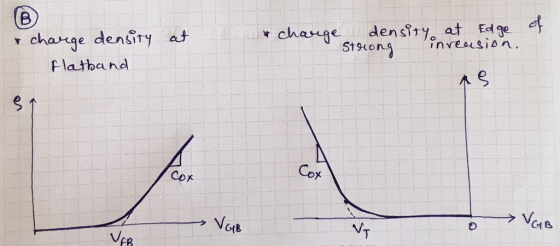
 Section B (total 60 marks for section B) B1 a) An MOS capacitor has a p-type semiconductor substrate doped with an impurity concentration of 1018 cm3. Assume a poly-Si material is used for the gate. Draw a diagram of the capacitor structure showing material types and an energy band diagram it is in thermal equilibrium. (10 marks) b) Given an MOS capacitor with a p-type semiconductor substrate and poly-Si material as gate (in part a), what is the meaning of...
Problem 3: Consider a MOS capacitor maintained at T= 300K with the following characteristics: Assume s 11.9, ox 3.9, 8.85x 10⁻¹ F/cm, and n 1.5 x 1010cm3 Gate material is n poly-silicon Total...
 Problem 3: Consider a MOS capacitor maintained at T= 300K with the following characteristics: Assume s 11.9, ox 3.9, 8.85x 10⁻¹ F/cm, and n 1.5 x 1010cm3 Gate material is n poly-silicon Total negative oxide charge of 5x 10¹¹q C/cm . Substrate is n-type Si, with doping concentration 1 x1016 cm-3 Oxide thickness 5 nmm The electron affinity for Si is 4.03eV? e) What is the flat capacitance? f) What is the depletion region width? g) What is the potential...
Problem 5: The gate capacitance vs. gate voltage characteristic of a p+ poly-Si gated MOS capacitor of area 1x10"cm', is as shown: Assume Esi = 11.9, Eox-39,E,-8.85 × 10⁻¹⁴ F/on, and nl =...
 Problem 5: The gate capacitance vs. gate voltage characteristic of a p+ poly-Si gated MOS capacitor of area 1x10"cm', is as shown: Assume Esi = 11.9, Eox-39,E,-8.85 × 10⁻¹⁴ F/on, and nl = 1.5 x 1010 cm3 Co [Farads] 3.45x10¹¹ >Va [Volts] 1.0 0.3 (a) Is the semiconductor (silicon) substrate doped n-type or p-type? Explain briefly. (b) Is the measurement frequency low or high? Explain briefly. (c) What is the thickness of the gate oxide (SiO2), xo? (d) Estimate the...
Q1 Which of the following is true for a MOS capacitor with a P-type body? Select...
Q1 Which of the following is true for a MOS capacitor with a P-type body? Select one: a. The charge in the inversion layer stays approximately constant as the gate voltage is increased above the threshold voltage b. The charge in the depletion region is proportional to the square root of the depletion region width, assuming that the body is uniformly doped c. In inversion, the total charge is equal to the sum of the charge in the depletion region...
 Consider an n-channel Silicon MOS system with a substrate resistivity of 10 0-cm and with a polycrystalline gate. Assume that the polysilicon gate is doped with boron atoms to a density of 1x1019 cm and that the silicon dioxide is 50 nm-thick. The channel is not biased except from the gate (Vc= VB = 0). (i) Accurately sketch the band diagram identifying flatband voltage, surface potential at inversion, depletion width at inversion, and charges at inversion. Tabulate these parameters. (ii)...
 Problem 3 (25 points) Consider a MOS capacitor with p polysilicon gate and p-type silicon substrate with NA 1016 cm3. Ef- Ev in the polysilicon gate. Assume the following parameters: I200A, , 1.5x10° cm*,E, -3.9x8.854x104FIcm ox a) (5 points) Calculate the metal-semiconductor work function difference. b) (5 points) Calculate the surface potential at the threshold inversion. c) (5 points) Calculate the depletion width (in μm) at the threshold inversion. d) (5 points) Calculate the flat band voltage. e) (5 points)...
 In the silicon-based n-channel MOSMET. the work function of gate electrode 4a 4.08eV and the electron affinity of silicon χ = 4.05eV. The fixed oxide charge located at Si-SiO2 interface has a density of 5x10¹⁴ m-2 . The silicon substrate is doped with boron atoms in a concentration of 2x10*°m3. The oxide layer has a thickness of 200nm. Calculate (i) the flat band voltage, (ii) the threshold voltage to induce the inversion layer and ii) the maximum, minimum and flat...
 Problem3: Consider a MOS capacitor maintained at T 300K with the following characteristics: Assume Esi 1.9,x 3.9,8.85 x 10-14 F/cm, and n 1.5 x 1010cm3 . Gate material is n+ poly-silicon . Total negative oxide charge of 5x 10¹¹q C/cnm2 . Substrate is n-type Si, with doping concentration 1x1016 cm3 Oxide thickness 5 nm . The electron affinity for Si is 4.03eV? a) Draw the band diagram at equilibrium. b) From part (a). What is the substrate (bulk) condition at...
 from Semiconductors class
2. An n-MOSFET has substrate doping N,-10°cm, oxide thickness ox-50 nm and n+ poly silicon gate. The oxide has fixed charge of 2 x10¹⁰/cm2 Cim 1. Calculate the flat band voltage VF Hint: fixed charge adjustsVby OIC 2. Threshold voltage V HINT
from Semiconductors class
2. An n-MOSFET has substrate doping N,-10°cm, oxide thickness ox-50 nm and n+ poly silicon gate. The oxide has fixed charge of 2 x10¹⁰/cm2 Cim 1. Calculate the flat band voltage VF Hint: fixed charge adjustsVby OIC 2. Threshold voltage V HINT
 6. A MOS system has an n+ polysilicon gate and a p-type silicon substrate doped to N. =10cm. Assume there is an oxide surface charge density (Q,/q) = 100cm 2. Design the oxide thickness so that V1 = 0.5 V (no bias is applied between the channel and substrate). Answer: x 58.5 nm OX
 Section B (total 60 marks for section B) B1 a) An MOS capacitor has a p-type semiconductor substrate doped with an impurity concentration of 1018 cm3. Assume a poly-Si material is used for the gate. Draw a diagram of the capacitor structure showing material types and an energy band diagram it is in thermal equilibrium. (10 marks) b) Given an MOS capacitor with a p-type semiconductor substrate and poly-Si material as gate (in part a), what is the meaning of...
 Problem 3: Consider a MOS capacitor maintained at T= 300K with the following characteristics: Assume s 11.9, ox 3.9, 8.85x 10⁻¹ F/cm, and n 1.5 x 1010cm3 Gate material is n poly-silicon Total negative oxide charge of 5x 10¹¹q C/cm . Substrate is n-type Si, with doping concentration 1 x1016 cm-3 Oxide thickness 5 nmm The electron affinity for Si is 4.03eV? e) What is the flat capacitance? f) What is the depletion region width? g) What is the potential...
 Problem 5: The gate capacitance vs. gate voltage characteristic of a p+ poly-Si gated MOS capacitor of area 1x10"cm', is as shown: Assume Esi = 11.9, Eox-39,E,-8.85 × 10⁻¹⁴ F/on, and nl = 1.5 x 1010 cm3 Co [Farads] 3.45x10¹¹ >Va [Volts] 1.0 0.3 (a) Is the semiconductor (silicon) substrate doped n-type or p-type? Explain briefly. (b) Is the measurement frequency low or high? Explain briefly. (c) What is the thickness of the gate oxide (SiO2), xo? (d) Estimate the...
Most questions answered within 3 hours.
-
Assume that a randomly selected subject is given a bone density
test. Those test scores are...
asked 1 minute ago -
Pretend that you are a developmental psychologist and the
superintendent for a school district in MA...
asked 1 minute ago -
If you add 4.00 mL of pure water to 6.00 mL of .750 M NaCl
solution,...
asked 20 minutes ago -
Mr. Lam had recently had a heart attack that caused a secondary
pericarditis, Dressler syndrome, with...
asked 7 minutes ago -
At 5 am your alarm goes off. Genes are expressed in response to
that stimulus and...
asked 22 minutes ago -
Why is the short-run Phillips curve downward sloping? Explain
the reasons behind the downward slope of...
asked 16 minutes ago -
Last year, sanitation engineer crews in Buffalo, New York,
collected 124 tons of trash per day....
asked 14 minutes ago -
Develop a MATLAB function that will compute the following
function. Test your function for t =...
asked 18 minutes ago -
Case study 2.1 : W.L GORE AND
ASSOCIATES
1. How did Bill Gore structure management within...
asked 20 minutes ago -
Convert 31 ft^2 to yd^2
Round your answer to two decimal places.
asked 18 minutes ago -
Question#4
Given the following 14 compounds: acetic acid ammonia sodium
chloride carbon dioxide water perchloric acid...
asked 44 minutes ago -
Antimony, Sb, has two stable isotopes: 121Sb, 120.904u, and
123Sb, 122.904u. What is the percent abundance...
asked 55 minutes ago