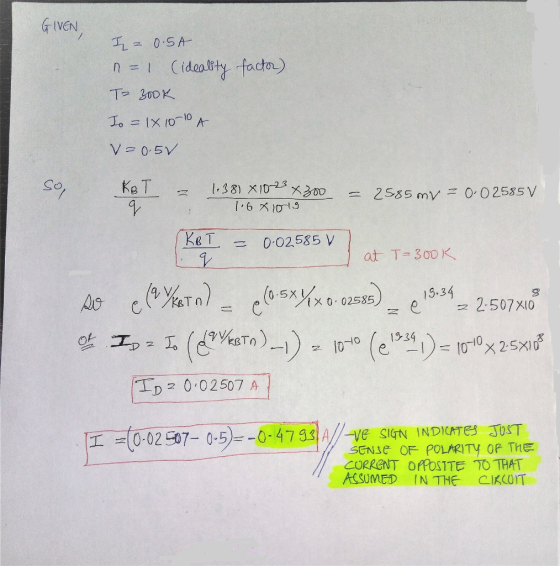
What is the current in A, from a PV cell if dark saturation current, I0(Insat) = 1.000x10⁻¹⁰A,...
What is the current in A, from a PV cell if dark saturation current, I0(Insat) = 1.000x10⁻¹⁰A, light generated current, IL= 0.500 A, ideality factor, n = 1, temperature, T = 300 K, and voltage, V = 0.500 V ? Express the result with 3 significant figures, include zero between the decimal point and do not write in the unit (it is already included in the question).
Homework Answers

CONCEPT:
IN THE ABOVE FIGURES , 1ST FIGURE TELLS YOU ABOUT BASIC CIRCUIT OF ANY PV CELL HAVING A PHOTODIODE RECIEVING RAYS OF SUN AND POWERING UP THE LOAD AT ITS OUTPUT .
2ND FIGURE IS EXPANDED MODEL OF PV CELL HAVING A CONSTANT CURRENT SOURCE IL WHICH SIGNIFIES ABOUT LIGHT GENERATED CURRENT , ALSO A DIODE IS IN PARALLEL CARRYING ID DIODE CURRENT .
NOW , BY KCL AT NODE A ,
I= ( ID - IL ) // CURRENT FROM PV CELL(AT OUTPUT)
Where, I= CURRENT DRAWN FROM PV CELL
IL= PHOTOCURRENT OR LIGHT GENRATED CURRENT
ID = DIODE CURRENT = I0 [e (qV / nKb T) - 1)
where further, I0 = DARK SATURATION CURRENT
q = electric charge unit = 1.602 * 10-19 C
V = voltage
kb = boltzman constant = 1.381 * 10-23 J/K
T = temprature in Kelvin
n = ideality factor
NOW COMING TO QUESTION SOLUTION ,
Add Answer to:
What is the current in A, from a PV cell if dark saturation
current, I0(Insat)
= 1.000x10⁻¹⁰A,...
What is the open circuit voltage in V, for a cell if dark saturation current, I0= 1.000...
What is the open circuit voltage in V, for a cell if dark saturation current, I0= 1.000 x10⁻¹⁰A , light generated current, IL= 0.500 A, ideality factor, n = 1, and temperature, T = 300 K? Fill in the result only, use 3 significant figures, use zero before the decimal point, do not write the unites
3- Draw a typical JV curve of a solar cell in the dark and under illumination...
 3- Draw a typical JV curve of a solar cell in the dark and under illumination condition. Specify open circuit voltage and short circuit current. Draw the generated power by that cell under illumination condition. [5 marks] 4- A solar cell has a dark saturation current density of jo = 10-18 A/cm². If the photo-current is 0.024 A/cm² what is the open circuit voltage of the solar cell at room temperature? What happens to open circuit voltage as the solar...
5) A Si solar cell with junction cross sectional dimensions 2 cm ×2 cmis formed with Na 1018 cm3 on the p side and Nd 1018cm3 on the n side. It is operated at a temperature of 300 K and τn-tp-1 μ. a)...
 5) A Si solar cell with junction cross sectional dimensions 2 cm ×2 cmis formed with Na 1018 cm3 on the p side and Nd 1018cm3 on the n side. It is operated at a temperature of 300 K and τn-tp-1 μ. a) Using the mobilities on the equation sheet, calculate the dark saturation current. b) An intrinsic region of thickness 200 μm is sandwiched between the p and n regions in order to enhance the active volume of the...
Review Constants The current shown in (Figure 1) is applied to a 350 nF capacitor. The...
 Review Constants The current shown in (Figure 1) is applied to a 350 nF capacitor. The initial voltage on the capacitor is zero. Part A Find the charge on the capacitor at t = 30 jus Express your answer to three significant figures and include the appropriate units. IT μΑ q= 25.103 O Submit Previous Answers Request Answer Part B Find the voltage on the capacitor at t = 50 js. Express your answer to three significant figures and include...
Review Con: Part A An incandescent light bulb uses a coiled filament of tungsten that is...
 Review Con: Part A An incandescent light bulb uses a coiled filament of tungsten that is 580 mm long with a diameter of 46.0 um. At 20.0°C tungsten has a resistivity of 5.25 x 1012.m. Its temperature coefficient of resistivity is 0.0045 (Cº) , and this remains accurate even at high temperatures. The temperature of the filament increases linearly with current, from 20°C when no current flows to 2520°C at 1.00 A of current What is the resistance of the...
A common source amplifier circuit based on a single n-channel MOSFET is shown in Figure 4b. Assume that the transconductance gm-60 mS (equivalent to mA/ V) and drain source resistance, os,...
 A common source amplifier circuit based on a single n-channel MOSFET is shown in Figure 4b. Assume that the transconductance gm-60 mS (equivalent to mA/ V) and drain source resistance, os, is so large it may be neglected. 0) Calculate the open circuit voltage gain Av Yout/ Vis. i) The amplifier has a load of 10 k2. Determine the current gain Va. = 12 V 150k 4k3 Vout Vin 200k GND = 0 V Figure 4b a) State the name...
Taking pure silicon (Si) as an example, explain what is meant by the terms electron-hole generation...
 Taking pure silicon (Si) as an example, explain what is meant by the terms electron-hole generation and recombination, how they affect the electrical conductivity, and define what is meant by the "intrinsic carrier density", n. [5 marks] Q3. a) b) With the aid of both lattice and energy band diagrams, explain how n-type doping of Si is achieved and state two types of suitable dopant atoms. [7 marks] c) An n-type region on a Si wafer has a donor concentration...
1. Figure G: The ideal battery has an emf of 14 V. What is the current...
 1. Figure G: The ideal battery has an emf of 14 V. What is the current (A) in R a) 0.200 D0.250 b) 1.00 g) 0.100 c)0.500 h)0.235 2. Figure C shows, in cross section, a spherical conducting shell that surrounds a particle of charge -2e. The shell d) 0.667 i) 1.23 e) 0.750 has a net charge of -6e. What is the magnitude (N/C) of the electric field at point P, at distance2.00 m from the j)0.820 center of...
Yes, this is one problem. Please solve ALL PARTS. Guaranteed thumbs up for the person who solves it. 3 1. Photodiode...
 Yes, this is one problem. Please solve ALL PARTS. Guaranteed
thumbs up for the person who solves it.
3 1. Photodiode amplifier circuit You are designinga CF photosensor circuit for a light detection and ranging LiDAR) system in autonomous vehicles. The circuit utilizes a transimpedance amplifier to convert low-level RF photodiode current signal to a usable voltage output. It consists of a photodiode, an amplifier, and feedback capacitor/resistor pair as shown in Figure 1. We will derive simple equations to...
Yes, this is one problem. Please solve ALL PARTS. Guaranteed
thumbs up for the person who solves it.
3 1. Photodiode amplifier circuit You are designinga CF photosensor circuit for a light detection and ranging LiDAR) system in autonomous vehicles. The circuit utilizes a transimpedance amplifier to convert low-level RF photodiode current signal to a usable voltage output. It consists of a photodiode, an amplifier, and feedback capacitor/resistor pair as shown in Figure 1. We will derive simple equations to...
Notes for lab dc02-Resistors and the Color Code will skip are Part 2 e, g: Part 4; Exercises 2, 4,5,6 an...
 Notes for lab dc02-Resistors and the Color Code will skip are Part 2 e, g: Part 4; Exercises 2, 4,5,6 and 3. It is important to answer the exercises correctly in each labl you should include the appropriate prefix for the unit in the Numerical Value We will not be Volt using the Volt-Ohm meter (VOM) for this lab, so skip the parts that ask for VOM measurements. The parts we You do need to complete Exercises1 Note that in...
 3- Draw a typical JV curve of a solar cell in the dark and under illumination condition. Specify open circuit voltage and short circuit current. Draw the generated power by that cell under illumination condition. [5 marks] 4- A solar cell has a dark saturation current density of jo = 10-18 A/cm². If the photo-current is 0.024 A/cm² what is the open circuit voltage of the solar cell at room temperature? What happens to open circuit voltage as the solar...
 5) A Si solar cell with junction cross sectional dimensions 2 cm ×2 cmis formed with Na 1018 cm3 on the p side and Nd 1018cm3 on the n side. It is operated at a temperature of 300 K and τn-tp-1 μ. a) Using the mobilities on the equation sheet, calculate the dark saturation current. b) An intrinsic region of thickness 200 μm is sandwiched between the p and n regions in order to enhance the active volume of the...
 Review Constants The current shown in (Figure 1) is applied to a 350 nF capacitor. The initial voltage on the capacitor is zero. Part A Find the charge on the capacitor at t = 30 jus Express your answer to three significant figures and include the appropriate units. IT μΑ q= 25.103 O Submit Previous Answers Request Answer Part B Find the voltage on the capacitor at t = 50 js. Express your answer to three significant figures and include...
 Review Con: Part A An incandescent light bulb uses a coiled filament of tungsten that is 580 mm long with a diameter of 46.0 um. At 20.0°C tungsten has a resistivity of 5.25 x 1012.m. Its temperature coefficient of resistivity is 0.0045 (Cº) , and this remains accurate even at high temperatures. The temperature of the filament increases linearly with current, from 20°C when no current flows to 2520°C at 1.00 A of current What is the resistance of the...
 A common source amplifier circuit based on a single n-channel MOSFET is shown in Figure 4b. Assume that the transconductance gm-60 mS (equivalent to mA/ V) and drain source resistance, os, is so large it may be neglected. 0) Calculate the open circuit voltage gain Av Yout/ Vis. i) The amplifier has a load of 10 k2. Determine the current gain Va. = 12 V 150k 4k3 Vout Vin 200k GND = 0 V Figure 4b a) State the name...
 Taking pure silicon (Si) as an example, explain what is meant by the terms electron-hole generation and recombination, how they affect the electrical conductivity, and define what is meant by the "intrinsic carrier density", n. [5 marks] Q3. a) b) With the aid of both lattice and energy band diagrams, explain how n-type doping of Si is achieved and state two types of suitable dopant atoms. [7 marks] c) An n-type region on a Si wafer has a donor concentration...
 1. Figure G: The ideal battery has an emf of 14 V. What is the current (A) in R a) 0.200 D0.250 b) 1.00 g) 0.100 c)0.500 h)0.235 2. Figure C shows, in cross section, a spherical conducting shell that surrounds a particle of charge -2e. The shell d) 0.667 i) 1.23 e) 0.750 has a net charge of -6e. What is the magnitude (N/C) of the electric field at point P, at distance2.00 m from the j)0.820 center of...
 Yes, this is one problem. Please solve ALL PARTS. Guaranteed
thumbs up for the person who solves it.
3 1. Photodiode amplifier circuit You are designinga CF photosensor circuit for a light detection and ranging LiDAR) system in autonomous vehicles. The circuit utilizes a transimpedance amplifier to convert low-level RF photodiode current signal to a usable voltage output. It consists of a photodiode, an amplifier, and feedback capacitor/resistor pair as shown in Figure 1. We will derive simple equations to...
Yes, this is one problem. Please solve ALL PARTS. Guaranteed
thumbs up for the person who solves it.
3 1. Photodiode amplifier circuit You are designinga CF photosensor circuit for a light detection and ranging LiDAR) system in autonomous vehicles. The circuit utilizes a transimpedance amplifier to convert low-level RF photodiode current signal to a usable voltage output. It consists of a photodiode, an amplifier, and feedback capacitor/resistor pair as shown in Figure 1. We will derive simple equations to...
 Notes for lab dc02-Resistors and the Color Code will skip are Part 2 e, g: Part 4; Exercises 2, 4,5,6 and 3. It is important to answer the exercises correctly in each labl you should include the appropriate prefix for the unit in the Numerical Value We will not be Volt using the Volt-Ohm meter (VOM) for this lab, so skip the parts that ask for VOM measurements. The parts we You do need to complete Exercises1 Note that in...
Most questions answered within 3 hours.
-
Instructions Part 1 - Implementation of a Doubly Linked
List Attached you will find the code...
asked 1 hour ago -
You work for a factory making bricks. A coworker accidentally
contaminated one of the bricks with...
asked 1 hour ago -
for python-3
I want to prompt the user to enter their first name and then
Call...
asked 2 hours ago -
Q3 If the formation of a hairpin loop requires a minimum
stem
length of 6 contiguous...
asked 2 hours ago -
Enzymes work by lowering the _____ of a reaction.
Select one:
a. activation energy
b. entropy...
asked 3 hours ago -
Assume three digits are used to represent positive integers and
also assume the following operations are...
asked 3 hours ago -
How many stairs can a 63-kg person climb up with the energy
contained in a candy...
asked 3 hours ago -
Problem 1
A 0.150 kg baseball pitched at 40.0 m/s is hit on a horizontal
line...
asked 3 hours ago -
Variance in reproductive success. The variance among male
reproductive success is 2 and the variance among...
asked 5 hours ago -
To decide your fate, you will play a board game on a simple
board: a linear...
asked 8 hours ago -
1. What are specialty engines? ( )
a. Logical Processors that perform specialized functions
b. An...
asked 8 hours ago -
a. What double precision floating point
number is represented by the following 64-bit binary? Show your...
asked 9 hours ago