Problem: The purpose of this lab is to introduce concepts of boolean logic reduction including the...
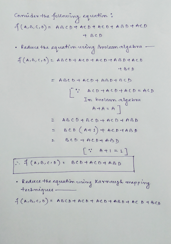
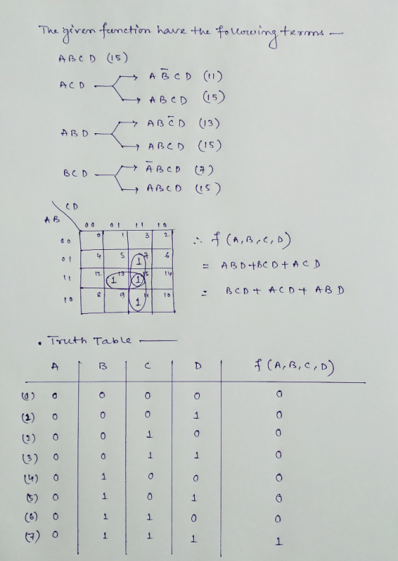
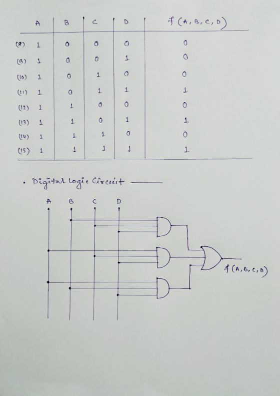
Problem: The purpose of this lab is to introduce concepts of boolean logic reduction including the use of boolean algebra reduction techniques as well as karnaugh map reduction techniques. Assignment: Consider the following equation: _ _ _ _ _ _ _ _ _ f(A,B,B,D) = A B C D + A C D + A C D + A B D + A C D + B C D For this equation, you will need to complete the following objectives: _____ Reduce the equation using boolean algebra (show all work) _____ Reduce the equation using karnaugh mapping techniques _____ Draw the truth table for this circuit _____ Draw the circuit diagram needed to implement this design _____ Build the digital circuit necessary to implement this logic Assessment This lab exercise consists of two assessment phases. Phase one requires the demonstration of your functioning circuit in lab to the lab instructor and phase two requires the submission of a lab report. The report should contain the following sections and all elements must be computer generated (no hand drawings of any kind). Your report should include: Cover sheet with your name, date, class, etc. Introduction explaining the lab purpose A section for each of the above objectives Demonstration Signoff Demo completed on ________ at time ________ Instructor signature: _______________________
Homework Answers
All the subparts of the given question have been solved with proper explanation.
Add Answer to:
Problem: The purpose of this lab is to introduce concepts of
boolean logic reduction including the...
the answer on the cheeg is not right. i want a new answer Problem: The purpose...
 the
answer on the cheeg is not right. i want a new answer
Problem: The purpose of this lab is to introduce concepts of boolean logic reduction including the use of boolean algebra reduction techniques as well as karnaugh map reduction techniques. Assignment: Consider the following equation: f(A,B,B,D)-ABCD ACDACD A BDACD BCD For this equation, you will need to complete the following objectives: Reduce the equation using boolean algebra (show all work) Reduce the equation using karnaugh mapping techniques Draw...
the
answer on the cheeg is not right. i want a new answer
Problem: The purpose of this lab is to introduce concepts of boolean logic reduction including the use of boolean algebra reduction techniques as well as karnaugh map reduction techniques. Assignment: Consider the following equation: f(A,B,B,D)-ABCD ACDACD A BDACD BCD For this equation, you will need to complete the following objectives: Reduce the equation using boolean algebra (show all work) Reduce the equation using karnaugh mapping techniques Draw...
Problem: The purpose of this lab is to explore combinational logic design and switch/LED interfacing techniques...
 Problem: The purpose of this lab is to explore combinational logic design and switch/LED interfacing techniques Assignment: Design a digital system that will count the number of switches activated and display that count in binary using LEDS. An LED that isilluminated represents a 1' and an LED that is off represents a 0'. Note that you may utilize ANY chips in your part kits to implement this design. For this design, you will need to complete the following objectives: Interface...
Using the Boolean logic expression below, draw circuit diagram with logic gates that will implement your...
 Using the Boolean logic expression below, draw circuit diagram with logic gates that will implement your Boolean expression without simplifying or expanding the expression. F(A, B, C, D) = ABD + ABCD + ABCD + ABCD Complete a Truth Table F(A, B, C, D). Use your logic circuit diagram and Boolean logic expression as much as possible.
Problem 1: consider the following circuit with 4 inputs A, B, c, D, and 3 outputs...
 Problem 1:
consider the following circuit with 4 inputs A, B, c, D, and 3 outputs F, G, H. Each input/output is connected to an input/output port. 3-input OR gate Figure 1 a) Determine the Boolean algebra equations relating each input to each output of the circuit. b) Create the truth tables corresponding to the equations obtained above. There should be one truth table per equation c) Produce the Karnaugh maps corresponding to the truth tables d) Determine simplified Boolean...
Problem 1:
consider the following circuit with 4 inputs A, B, c, D, and 3 outputs F, G, H. Each input/output is connected to an input/output port. 3-input OR gate Figure 1 a) Determine the Boolean algebra equations relating each input to each output of the circuit. b) Create the truth tables corresponding to the equations obtained above. There should be one truth table per equation c) Produce the Karnaugh maps corresponding to the truth tables d) Determine simplified Boolean...
8).- The logic circuit shown is used to turn on a warning buzzer at X based...
 8).- The logic circuit shown is used to turn on a warning buzzer at X based on the input conditions at A, B, C and D. A simplified equivalent circuit that will perform the same function can be formed by using Boolean algebra and D'Morgan's Theorem. 1).- Write the Boolean equation of the circuit 2. Simplify the equation using Boolean Algebra and D'Morgan's Theorem. 3. Draw the logie circuit of the simplified equation (Hint: We using 4 Gates to build...
Derive the Boolean expression of a combination logic from the following truth table, where A, B,...
 Derive the Boolean expression of a combination logic from the following truth table, where A, B, C are input variables and D is output. Draw the circuit diagram to implement it. Show your working steps. The full subtractor is a combinational circuit, which is used to perform subtraction of three input bits: the minuend X, subtrahend Y, and borrow in B_in. The full subtractor generates two outputs bits: the difference D and borrow out B_out. B_in is set when the...
Logic Circuits Lab Project ELEG 3021 2018 Fall Obiective: Given a practical problem, using the knowledge...
 Logic Circuits Lab Project ELEG 3021 2018 Fall Obiective: Given a practical problem, using the knowledge learned in Logic Circuit class and practical skills gained in the Logic Circuit Lab, develop and conduct appropriate experimentation, analyze and interpret data, and use engineering judgment to draw conclusions. Problem: Given any two unsigned 4-bit numbers A (AsA2AiAo) and B (B;B B Bo), please compare the magnitude of this two numbers and pass the larger one of the two to the output Y...
please anwer all the part of this lab and please use multisim. Lab 4: Basic Logic...
 please anwer all the part of this lab and please use
multisim.
Lab 4: Basic Logic Gates and Multisim Tools Objectives: • Learn to use the Logic Converter in Multisim to generate truth tables, design circuits and simplify logic expressions. • Build logic circuits using basic TTL gates. Software and Materials: • Multisim One 7400 (quad 2-input NAND gate) IC chip Procedure: 1. Write a logic expression for the circuit below. Have your instructor check the expression. А B с...
please anwer all the part of this lab and please use
multisim.
Lab 4: Basic Logic Gates and Multisim Tools Objectives: • Learn to use the Logic Converter in Multisim to generate truth tables, design circuits and simplify logic expressions. • Build logic circuits using basic TTL gates. Software and Materials: • Multisim One 7400 (quad 2-input NAND gate) IC chip Procedure: 1. Write a logic expression for the circuit below. Have your instructor check the expression. А B с...
Lab problem description: A register cell is to be designed for an 8-bit register RO that...
 Lab problem description: A register cell is to be designed for an 8-bit register RO that has the following Register Transfer Functions (Registers RO and R1 serve as the 8-bit sources) Prelab: a) Draw the block diagram for the implementation of the Register Transfer Functions listed above b) Draw the logic diagram (for one bit) of the hardware implementation (of the Register Transfer Functions listed above) by using functional block symbols for the registers (RO and RI) and using a...
At this point in your Digital Logic career, an assignment comes where you need to put all your knowledge of J-K flip-flops
At this point in your Digital Logic career, an assignment comes where you need to put all your knowledge of J-K flip-flops, counters and shift registers together and design, build and test a circuit that will detect a "101" pattern in a serial bit stream and output a HIGH level coincident with the final "1" in the pattern, Using A Qty. of 2, J-K Flip-Flops 1) Create a State diagram defining the operational states of your pattern detector 2) Draw a schematic...
 the
answer on the cheeg is not right. i want a new answer
Problem: The purpose of this lab is to introduce concepts of boolean logic reduction including the use of boolean algebra reduction techniques as well as karnaugh map reduction techniques. Assignment: Consider the following equation: f(A,B,B,D)-ABCD ACDACD A BDACD BCD For this equation, you will need to complete the following objectives: Reduce the equation using boolean algebra (show all work) Reduce the equation using karnaugh mapping techniques Draw...
the
answer on the cheeg is not right. i want a new answer
Problem: The purpose of this lab is to introduce concepts of boolean logic reduction including the use of boolean algebra reduction techniques as well as karnaugh map reduction techniques. Assignment: Consider the following equation: f(A,B,B,D)-ABCD ACDACD A BDACD BCD For this equation, you will need to complete the following objectives: Reduce the equation using boolean algebra (show all work) Reduce the equation using karnaugh mapping techniques Draw...
 Problem: The purpose of this lab is to explore combinational logic design and switch/LED interfacing techniques Assignment: Design a digital system that will count the number of switches activated and display that count in binary using LEDS. An LED that isilluminated represents a 1' and an LED that is off represents a 0'. Note that you may utilize ANY chips in your part kits to implement this design. For this design, you will need to complete the following objectives: Interface...
 Using the Boolean logic expression below, draw circuit diagram with logic gates that will implement your Boolean expression without simplifying or expanding the expression. F(A, B, C, D) = ABD + ABCD + ABCD + ABCD Complete a Truth Table F(A, B, C, D). Use your logic circuit diagram and Boolean logic expression as much as possible.
 Problem 1:
consider the following circuit with 4 inputs A, B, c, D, and 3 outputs F, G, H. Each input/output is connected to an input/output port. 3-input OR gate Figure 1 a) Determine the Boolean algebra equations relating each input to each output of the circuit. b) Create the truth tables corresponding to the equations obtained above. There should be one truth table per equation c) Produce the Karnaugh maps corresponding to the truth tables d) Determine simplified Boolean...
Problem 1:
consider the following circuit with 4 inputs A, B, c, D, and 3 outputs F, G, H. Each input/output is connected to an input/output port. 3-input OR gate Figure 1 a) Determine the Boolean algebra equations relating each input to each output of the circuit. b) Create the truth tables corresponding to the equations obtained above. There should be one truth table per equation c) Produce the Karnaugh maps corresponding to the truth tables d) Determine simplified Boolean...
 8).- The logic circuit shown is used to turn on a warning buzzer at X based on the input conditions at A, B, C and D. A simplified equivalent circuit that will perform the same function can be formed by using Boolean algebra and D'Morgan's Theorem. 1).- Write the Boolean equation of the circuit 2. Simplify the equation using Boolean Algebra and D'Morgan's Theorem. 3. Draw the logie circuit of the simplified equation (Hint: We using 4 Gates to build...
 Derive the Boolean expression of a combination logic from the following truth table, where A, B, C are input variables and D is output. Draw the circuit diagram to implement it. Show your working steps. The full subtractor is a combinational circuit, which is used to perform subtraction of three input bits: the minuend X, subtrahend Y, and borrow in B_in. The full subtractor generates two outputs bits: the difference D and borrow out B_out. B_in is set when the...
 Logic Circuits Lab Project ELEG 3021 2018 Fall Obiective: Given a practical problem, using the knowledge learned in Logic Circuit class and practical skills gained in the Logic Circuit Lab, develop and conduct appropriate experimentation, analyze and interpret data, and use engineering judgment to draw conclusions. Problem: Given any two unsigned 4-bit numbers A (AsA2AiAo) and B (B;B B Bo), please compare the magnitude of this two numbers and pass the larger one of the two to the output Y...
 please anwer all the part of this lab and please use
multisim.
Lab 4: Basic Logic Gates and Multisim Tools Objectives: • Learn to use the Logic Converter in Multisim to generate truth tables, design circuits and simplify logic expressions. • Build logic circuits using basic TTL gates. Software and Materials: • Multisim One 7400 (quad 2-input NAND gate) IC chip Procedure: 1. Write a logic expression for the circuit below. Have your instructor check the expression. А B с...
please anwer all the part of this lab and please use
multisim.
Lab 4: Basic Logic Gates and Multisim Tools Objectives: • Learn to use the Logic Converter in Multisim to generate truth tables, design circuits and simplify logic expressions. • Build logic circuits using basic TTL gates. Software and Materials: • Multisim One 7400 (quad 2-input NAND gate) IC chip Procedure: 1. Write a logic expression for the circuit below. Have your instructor check the expression. А B с...
 Lab problem description: A register cell is to be designed for an 8-bit register RO that has the following Register Transfer Functions (Registers RO and R1 serve as the 8-bit sources) Prelab: a) Draw the block diagram for the implementation of the Register Transfer Functions listed above b) Draw the logic diagram (for one bit) of the hardware implementation (of the Register Transfer Functions listed above) by using functional block symbols for the registers (RO and RI) and using a...
Most questions answered within 3 hours.
-
Accent Software faces the following conditions. All of these
support Accent’s use of a market-penetration pricing...
asked 38 minutes ago -
A mathematically inclined friend emails you the following
instructions: "Meet me in the cafeteria the first...
asked 40 minutes ago -
A monopoly sells in two countries . The demand curves in the two
countries are p1...
asked 1 hour ago -
A .15kg rubber ball is bounced off a wall. Before hitting the
wall, the ball moves...
asked 2 hours ago -
A manufacturing company preparing to build a new plant is
considering three potential locations for it....
asked 2 hours ago -
B. If compound Y has approximately the same values of solubility
in toluene as compound X,...
asked 3 hours ago -
Oscar Inc. has inventory in Japan valued at 39,051,000 Yen one
year ago. One year ago...
asked 3 hours ago -
If Canada suffered from "fundamental disequilibrium," and its
government choose not to devalue its currency, a...
asked 3 hours ago -
4. How many input & output Key Value Pairs are passed into,
and emitted out of...
asked 3 hours ago -
Why would your heart not function well if constructed of
skeletal muscle? What is the particular...
asked 3 hours ago -
Please respond to this essay question in full essay form for
Chemistry 1102 Organic and Biochemistry:...
asked 3 hours ago -
Determine the head loss and velocity of flow in a water supply main
of 15.0 cm...
asked 3 hours ago