Explain a frequency divider circuit using JK Flip-Flop. (In bullet form)
Explain a frequency divider circuit using JK Flip-Flop. (In bullet form)
Homework Answers


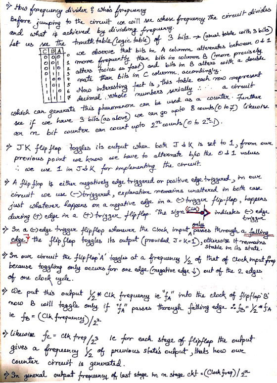

Therefore if you give a clock frequency (Clk) of say 8 MHz as input then the fC ( or QC ) will be 8 / 23 = 1 MHz.
Add Answer to:
Explain a frequency divider circuit using JK Flip-Flop. (In
bullet form)
I NEED HELP WITH FLIP FLOPS Flip-flop type JK Design a JK flip flop using only...
I NEED HELP WITH FLIP FLOPS Flip-flop type JK Design a JK flip flop using only logic gates .Fill the truth table exercising all possible combinations of inputs for J and K Flip-flop type D Set the JK type flip flop from the previous step to work as a flip flop type D. Fill the truth table by exercising all combinations of possible entries D Flip-flop type T Set the circuit of the previous step to work as a flip...
need it Circuit 1 (JK Flip Flop): (a) Simulate on Multisim a JK Flip Flop that makes use of a single D Flip Flop plus any necessary additional gates. (b)Physically build the JK Flip Flop of part (...
 need it
Circuit 1 (JK Flip Flop): (a) Simulate on Multisim a JK Flip Flop that makes use of a single D Flip Flop plus any necessary additional gates. (b)Physically build the JK Flip Flop of part (a) on the CADET.
Circuit 1 (JK Flip Flop): (a) Simulate on Multisim a JK Flip Flop that makes use of a single D Flip Flop plus any necessary additional gates. (b)Physically build the JK Flip Flop of part (a) on the CADET.
need it
Circuit 1 (JK Flip Flop): (a) Simulate on Multisim a JK Flip Flop that makes use of a single D Flip Flop plus any necessary additional gates. (b)Physically build the JK Flip Flop of part (a) on the CADET.
Circuit 1 (JK Flip Flop): (a) Simulate on Multisim a JK Flip Flop that makes use of a single D Flip Flop plus any necessary additional gates. (b)Physically build the JK Flip Flop of part (a) on the CADET.
A) Draw a frequency divider "divide by 2" and "divide by 4" logic circuits as a...
 A) Draw a frequency divider "divide by 2" and
"divide by 4" logic circuits as a single circuit utilizing JK
Flip-Flops. Indicate the input and output values on each
connection. Draw JK flip-flops as block
structures. Use rising edge triggering.
B) Draw your drawn JK Flip
Flop frequency divider circuit's outputs waveform to the
are below. Use rising edge triggering.
C) Draw a frequency divider "divide by 2" and
"divide by 4" logic circuits as a single circuit utilizing JK...
A) Draw a frequency divider "divide by 2" and
"divide by 4" logic circuits as a single circuit utilizing JK
Flip-Flops. Indicate the input and output values on each
connection. Draw JK flip-flops as block
structures. Use rising edge triggering.
B) Draw your drawn JK Flip
Flop frequency divider circuit's outputs waveform to the
are below. Use rising edge triggering.
C) Draw a frequency divider "divide by 2" and
"divide by 4" logic circuits as a single circuit utilizing JK...
At the gate level, draw the circuit diagram for a negative edge triggered JK flip flop....
At the gate level, draw the circuit diagram for a negative edge triggered JK flip flop. Briefly explain how your design can be modified to create a Positive Edge triggered T flip flop.
4.16 The circuit of Fig. P4.16a contains a JK flip-flop and a D flip-flop. Complete the...
 4.16 The circuit of Fig. P4.16a contains a JK flip-flop and a D flip-flop. Complete the timing diagram of Fig. P4.16b by drawing the waveforms of signals and Q. oc Lep roc Clock bs Clock__ CRU 2 Figure P4.16: a. Logic diagram. B. Timing diagram.
Design a 5-bit binary counter using JK flip flops. Draw the flip-flop circuit diagram, the state...
Design a 5-bit binary counter using JK flip flops. Draw the flip-flop circuit diagram, the state graph, the timing diagram, the truth table (with clk pulse) and the state table (with present and next states).
Procedure Using the test board, one 7476 Dual JK Flip-Flop chip and a function generator, connect...
 Procedure Using the test board, one 7476 Dual JK Flip-Flop chip and a function generator, connect the circuit shown in Fig-2. The inputs S, R, J and K must be connected to switches, while input C is connected to the function generator to implement the various cases of the inputs. Adjust the function generator to output a 2.5V-peak square wave with a DC offset 2.5V and a 100Hz frequency. Connect the outputs to LEDs. Connect the circuit to the power...
Configure a JK flip flop to act as a 'T' flip flop and complete th p...
 Configure a JK flip flop to act as a 'T' flip flop and complete th p to act as a 'T' flip flop and complete the logic diagram below for based on four pulses created win the pusa Duwon, with I held high, assuming starts at 0. Cik Research Question to be answered in the lab notebook: Looking at the waveforms just completed, while the flip flop is toggling w relationship of the frequency of Q to the frequency of...
Q5: 1. Design the circuit of JK Flip-Flop using DFF and derive state table and characteristic...
 Q5: 1. Design the circuit of JK Flip-Flop using DFF and derive state table and characteristic equation. 2. Draw the circuit of T Flip-Flop using JK FF and derive state table and characteristic equation. 3. For this SC derive the following • Derive Input Equations. • Derive Output Equation. • Derive State Equations. • Derive State Table • Design the State Diagram. 4. Suppose that a building with 4 floors (0-3), the task is to design a counter for an...
 need it
Circuit 1 (JK Flip Flop): (a) Simulate on Multisim a JK Flip Flop that makes use of a single D Flip Flop plus any necessary additional gates. (b)Physically build the JK Flip Flop of part (a) on the CADET.
Circuit 1 (JK Flip Flop): (a) Simulate on Multisim a JK Flip Flop that makes use of a single D Flip Flop plus any necessary additional gates. (b)Physically build the JK Flip Flop of part (a) on the CADET.
need it
Circuit 1 (JK Flip Flop): (a) Simulate on Multisim a JK Flip Flop that makes use of a single D Flip Flop plus any necessary additional gates. (b)Physically build the JK Flip Flop of part (a) on the CADET.
Circuit 1 (JK Flip Flop): (a) Simulate on Multisim a JK Flip Flop that makes use of a single D Flip Flop plus any necessary additional gates. (b)Physically build the JK Flip Flop of part (a) on the CADET.
 A) Draw a frequency divider "divide by 2" and
"divide by 4" logic circuits as a single circuit utilizing JK
Flip-Flops. Indicate the input and output values on each
connection. Draw JK flip-flops as block
structures. Use rising edge triggering.
B) Draw your drawn JK Flip
Flop frequency divider circuit's outputs waveform to the
are below. Use rising edge triggering.
C) Draw a frequency divider "divide by 2" and
"divide by 4" logic circuits as a single circuit utilizing JK...
A) Draw a frequency divider "divide by 2" and
"divide by 4" logic circuits as a single circuit utilizing JK
Flip-Flops. Indicate the input and output values on each
connection. Draw JK flip-flops as block
structures. Use rising edge triggering.
B) Draw your drawn JK Flip
Flop frequency divider circuit's outputs waveform to the
are below. Use rising edge triggering.
C) Draw a frequency divider "divide by 2" and
"divide by 4" logic circuits as a single circuit utilizing JK...
 4.16 The circuit of Fig. P4.16a contains a JK flip-flop and a D flip-flop. Complete the timing diagram of Fig. P4.16b by drawing the waveforms of signals and Q. oc Lep roc Clock bs Clock__ CRU 2 Figure P4.16: a. Logic diagram. B. Timing diagram.
 Procedure Using the test board, one 7476 Dual JK Flip-Flop chip and a function generator, connect the circuit shown in Fig-2. The inputs S, R, J and K must be connected to switches, while input C is connected to the function generator to implement the various cases of the inputs. Adjust the function generator to output a 2.5V-peak square wave with a DC offset 2.5V and a 100Hz frequency. Connect the outputs to LEDs. Connect the circuit to the power...
 Configure a JK flip flop to act as a 'T' flip flop and complete th p to act as a 'T' flip flop and complete the logic diagram below for based on four pulses created win the pusa Duwon, with I held high, assuming starts at 0. Cik Research Question to be answered in the lab notebook: Looking at the waveforms just completed, while the flip flop is toggling w relationship of the frequency of Q to the frequency of...
 Q5: 1. Design the circuit of JK Flip-Flop using DFF and derive state table and characteristic equation. 2. Draw the circuit of T Flip-Flop using JK FF and derive state table and characteristic equation. 3. For this SC derive the following • Derive Input Equations. • Derive Output Equation. • Derive State Equations. • Derive State Table • Design the State Diagram. 4. Suppose that a building with 4 floors (0-3), the task is to design a counter for an...
Most questions answered within 3 hours.
-
What are the negative effects of abruptly stopping the use of
all fossil fuels? Give at...
asked 1 minute from now -
Given that many conflict are the result of different parties having
different interests, is it possible...
asked 3 minutes ago -
A 750 g block can slide uniformly along the horizontal track
when a string attached to...
asked 6 minutes ago -
In 2017, Juan entered into a contract to write a book. The
publisher advanced Juan $50,000,...
asked 19 minutes ago -
Determine the number of kinds of protons in each molecule (w/
respect to NMR spectroscopy). Drawing...
asked 30 minutes ago -
A jeweler whose near point is 68 cm from his eye uses a
magnifying glass as...
asked 28 minutes ago -
A company wants to determine how many units of each of two
products, A and B,...
asked 32 minutes ago -
The blood pressure of a person changes throughout the day.
Suppose the systolic blood pressure of...
asked 40 minutes ago -
A chemistry student desired to study sulfur. Sulfur exhibited
the following characteristics with oxygen:
(a) It...
asked 36 minutes ago -
An Atwood machine is constructed of a solid-disk frictionless
pulley of mass m3 and radius R....
asked 38 minutes ago -
what are the advantages of lanthanum hexaboride over tungsten
filament for electron emission
what is the...
asked 39 minutes ago -
Question 5
Your uncle offers to sell you his vintage Rolls Royce. He
suggests a payment...
asked 44 minutes ago