Homework Answers


Add Answer to:
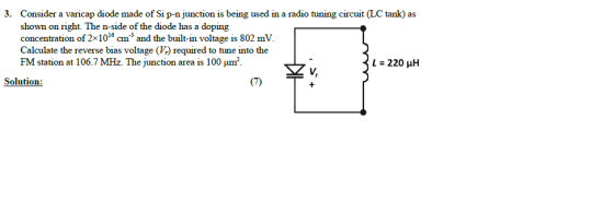
3. Consider a varicap diode made of Si p-n junction is being used in a radio tuning circuit (LC t...
1. Consider a p-n junction diode with doping concentrations: NA6.5x1015 cm3 and ND 107 cm3 in...
 1. Consider a p-n junction diode with doping concentrations: NA6.5x1015 cm3 and ND 107 cm3 in the p- and n-sides, respectively. (a) Calculate the free electron and hole concentrations in both p- and n-sides' neutral regions. (b) Find the barrier height and the built-in voltage. (c) Sketch the energy band diagram of the complete p-n junction. Mark all energy levels including the barrier height and show the energy level values. (d) Calculate the total depletion width under zero bias. (e)...
The doping and geometric parameters of a P–N junction diode are: - ND = 10^20 cm−3,...
The doping and geometric parameters of a P–N junction diode are: - ND = 10^20 cm−3, Wcathode = 1 μm <<Lp, - NA = 5 × 10^15 cm−3, Wanode = 10 μm <<Ln, - Junction area AJ = 500 × 500 μm2. Calculate the reverse biasing current IS, and then use this result to obtain the forward voltage that corresponds to a current of 100 mA, if the semiconductor material is: (a) Si (μn = 1450 cm2/V · s, μp...
Problem 4: Narrow-Base Diode Consider an ideal pn* step-junction Si diode maintained at 300K with cross-sectional...
 Problem 4: Narrow-Base Diode Consider an ideal pn* step-junction Si diode maintained at 300K with cross-sectional area A = 104cm2. The doping concentration on the p-type side is Na= 1017 cm3 (uncompensated). (The n-type side is degenerately doped.) The electron recombination lifetime in the p-type region is tn = 10-6 s. The width of the quasi-neutral p-type region is 1 um, for VA=0 V. a Is this a narrow-base diode? Justify your answer. b) Calculate the diode saturation current Io....
Problem 4: An abrupt silicon p-n junction diode has the following characteristics. side n-side N-4x 1016cm N1016cm3 n 1000 cm2/V sec 350 cm2/V sec Area A 102cm2 Calculate the following quantities...
 Problem 4: An abrupt silicon p-n junction diode has the following characteristics. side n-side N-4x 1016cm N1016cm3 n 1000 cm2/V sec 350 cm2/V sec Area A 102cm2 Calculate the following quantities: (a) Reverse saturation hole current component (b) Reverse saturation electron current component. (c) Minority carrier concentrations at the edge of the depletion layer, p(0) and pr(0), for a forward voltage of 0.6 V (d) Electron and hole current for the bias condition of (c). (e) Make a rough sketch...
1. Consider a p*n silicon diode at T-300 K with doping concentrations of N 10 cin...
 1. Consider a p*n silicon diode at T-300 K with doping concentrations of N 10 cin and N-101 cm-3. The minority carier hole diffusion coefficient is D 12 cm2/s and the minority carrier hole lifetime is po 10-7 s. The cross sectional area is A 10- cm2. Calculate the reverse saturation current and the diode current at a forward-bias voltage of 0.50v A germanium p* n diode at T-300 K has the following parameters: Na 108 cm-3 N,--1016 cm", ,...
Biased Si p-n junction (a) An abrupt Si p-n junction (Schottky model) of square cross section with area of 1x10⁻⁴ cm* has the following properties at 300 K: side Na - 1x1017 cm3 n side Na=1x10¹⁵ -3 c...
 Biased Si p-n junction (a) An abrupt Si p-n junction (Schottky model) of square cross section with area of 1x10⁻⁴ cm* has the following properties at 300 K: side Na - 1x1017 cm3 n side Na=1x10¹⁵ -3 cim =10us 200 cm 2/Vs) In 700 cm2/(Vs) In = 1300 cm 2/(Vs - 450 cm/(Vs) The junction is forward biased by 0.5 V. What is the forward current? (b) What is the current at a reverse bias of-0.5 V?
Biased Si p-n...
Biased Si p-n junction (a) An abrupt Si p-n junction (Schottky model) of square cross section with area of 1x10⁻⁴ cm* has the following properties at 300 K: side Na - 1x1017 cm3 n side Na=1x10¹⁵ -3 cim =10us 200 cm 2/Vs) In 700 cm2/(Vs) In = 1300 cm 2/(Vs - 450 cm/(Vs) The junction is forward biased by 0.5 V. What is the forward current? (b) What is the current at a reverse bias of-0.5 V?
Biased Si p-n...
3.13 Si pn junction Consider a long pn junction diode with an acceptor doping Naof 1018 cm-3 on t...
 3.13 Si pn junction Consider a long pn junction diode with an acceptor doping Naof 1018 cm-3 on the p-side and donor concentration of Nj on the n-side. The diode is forward biased and has a voltage of 0.6 V across it. The diode cross-sectional area is 1 mm2. The minority carrier recombination time, T, depends on the total dopant concentration, Ndopant (cm), through the following approximate empirical relation (5x 10⁻⁷)/(1 + 2 10-17N1°pan.) where T is in seconds. (a)...
Design an abrupt Si p+-n junction diode that has a reverse breakdown voltage of 130 V and has a forward-bias current of 2.2 mA at V = 0.7 volt. Assume tp = l0^-7 s.
Design an abrupt Sip+-n junction diode that has a reverse breakdown voltage of 130 V andhas a forward-bias current of 2.2 mA at V = 0.7 volt. Assume tp = l0^-7 s.
Consider a silicon pn step junction diode with NA-1x1018 cm3 and No 1x1017cm-3, maintained at T...
 Consider a silicon pn step junction diode with NA-1x1018 cm3 and No 1x1017cm-3, maintained at T 300K. The minority carrier lifetimes in the p-side and n-side are τη-10-8 s and Tp-10-7 s, respectively. a) Calculate the minority carrier densities at the edges of the depletion region when the applied voltage (VA) is 0.6 V. of the junction, for the applied bias voltage of part (a) densities are equal in magnitude, for the applied voltage of part (a). b) Sketch the...
p-side remain unchanged. 3. Consider a long silicon pn junction photodiode at T-300 K with the...
 p-side remain unchanged. 3. Consider a long silicon pn junction photodiode at T-300 K with the following parameters :N, 2x1016 cm-3,Nd-2x1 O18 cm's D,-25 crnVs, D,-10 cm?/sMr-2x10 po-10's. Assume a reverse bias voltage of VR-5 V is applied and assume a uniform generation rate of GL-1021 cm's-1 exists throughout the entire photodiode. Calculate the ratio of the prompt photocurrent density to the total steady state photocurrent density
 1. Consider a p-n junction diode with doping concentrations: NA6.5x1015 cm3 and ND 107 cm3 in the p- and n-sides, respectively. (a) Calculate the free electron and hole concentrations in both p- and n-sides' neutral regions. (b) Find the barrier height and the built-in voltage. (c) Sketch the energy band diagram of the complete p-n junction. Mark all energy levels including the barrier height and show the energy level values. (d) Calculate the total depletion width under zero bias. (e)...
 Problem 4: Narrow-Base Diode Consider an ideal pn* step-junction Si diode maintained at 300K with cross-sectional area A = 104cm2. The doping concentration on the p-type side is Na= 1017 cm3 (uncompensated). (The n-type side is degenerately doped.) The electron recombination lifetime in the p-type region is tn = 10-6 s. The width of the quasi-neutral p-type region is 1 um, for VA=0 V. a Is this a narrow-base diode? Justify your answer. b) Calculate the diode saturation current Io....
 Problem 4: An abrupt silicon p-n junction diode has the following characteristics. side n-side N-4x 1016cm N1016cm3 n 1000 cm2/V sec 350 cm2/V sec Area A 102cm2 Calculate the following quantities: (a) Reverse saturation hole current component (b) Reverse saturation electron current component. (c) Minority carrier concentrations at the edge of the depletion layer, p(0) and pr(0), for a forward voltage of 0.6 V (d) Electron and hole current for the bias condition of (c). (e) Make a rough sketch...
 1. Consider a p*n silicon diode at T-300 K with doping concentrations of N 10 cin and N-101 cm-3. The minority carier hole diffusion coefficient is D 12 cm2/s and the minority carrier hole lifetime is po 10-7 s. The cross sectional area is A 10- cm2. Calculate the reverse saturation current and the diode current at a forward-bias voltage of 0.50v A germanium p* n diode at T-300 K has the following parameters: Na 108 cm-3 N,--1016 cm", ,...
 Biased Si p-n junction (a) An abrupt Si p-n junction (Schottky model) of square cross section with area of 1x10⁻⁴ cm* has the following properties at 300 K: side Na - 1x1017 cm3 n side Na=1x10¹⁵ -3 cim =10us 200 cm 2/Vs) In 700 cm2/(Vs) In = 1300 cm 2/(Vs - 450 cm/(Vs) The junction is forward biased by 0.5 V. What is the forward current? (b) What is the current at a reverse bias of-0.5 V?
Biased Si p-n...
Biased Si p-n junction (a) An abrupt Si p-n junction (Schottky model) of square cross section with area of 1x10⁻⁴ cm* has the following properties at 300 K: side Na - 1x1017 cm3 n side Na=1x10¹⁵ -3 cim =10us 200 cm 2/Vs) In 700 cm2/(Vs) In = 1300 cm 2/(Vs - 450 cm/(Vs) The junction is forward biased by 0.5 V. What is the forward current? (b) What is the current at a reverse bias of-0.5 V?
Biased Si p-n...
 3.13 Si pn junction Consider a long pn junction diode with an acceptor doping Naof 1018 cm-3 on the p-side and donor concentration of Nj on the n-side. The diode is forward biased and has a voltage of 0.6 V across it. The diode cross-sectional area is 1 mm2. The minority carrier recombination time, T, depends on the total dopant concentration, Ndopant (cm), through the following approximate empirical relation (5x 10⁻⁷)/(1 + 2 10-17N1°pan.) where T is in seconds. (a)...
 Consider a silicon pn step junction diode with NA-1x1018 cm3 and No 1x1017cm-3, maintained at T 300K. The minority carrier lifetimes in the p-side and n-side are τη-10-8 s and Tp-10-7 s, respectively. a) Calculate the minority carrier densities at the edges of the depletion region when the applied voltage (VA) is 0.6 V. of the junction, for the applied bias voltage of part (a) densities are equal in magnitude, for the applied voltage of part (a). b) Sketch the...
 p-side remain unchanged. 3. Consider a long silicon pn junction photodiode at T-300 K with the following parameters :N, 2x1016 cm-3,Nd-2x1 O18 cm's D,-25 crnVs, D,-10 cm?/sMr-2x10 po-10's. Assume a reverse bias voltage of VR-5 V is applied and assume a uniform generation rate of GL-1021 cm's-1 exists throughout the entire photodiode. Calculate the ratio of the prompt photocurrent density to the total steady state photocurrent density
Most questions answered within 3 hours.
-
Write a program to solve the Josephus problem, with the following
modification:
Sample Input:
./a.out n...
asked 43 minutes ago -
At the start of a CD it is spinning at a rate of 525 rpm
(revolutions...
asked 1 hour ago -
4. Without doing any calculations, predict whether the observed
∆T would increase, decrease or remain the...
asked 2 hours ago -
Based on the range, which of the following sets of scores has
the greatest variability? 3,...
asked 3 hours ago -
Ripples in a pond travel at a velocity of 3 m/s with one peak
passing a...
asked 3 hours ago -
A man stands on the roof of a building of height 13.0 mm and
throws a...
asked 3 hours ago -
The extent to which assets are financed by borrowed funds and
other liabilities is indicated by:...
asked 4 hours ago -
Explain in detail
Germany is the fifth largest economy
explain what goods and services Germany specializes...
asked 4 hours ago -
The density of platinum is 21.45 g/mL. If a cube of platinum
with a mass of...
asked 4 hours ago -
Accounts Receivable
Sales
A/R Posting
Extended Sales Invoice
Packing Slip
Compare invoice to packing slip 2...
asked 5 hours ago -
Michaella, age 23, is a full-time law student and is claimed by
her parents as a...
asked 5 hours ago -
Why are polymers not typically casted into products?
asked 5 hours ago