
Homework Answers
Add Answer to:
Problem 4: Narrow-Base Diode Consider an ideal pn* step-junction Si diode maintained at 300K with cross-sectional...
this is a problem of semiconductor device and fundamentals. Problem 4: pn Junction Current Distributions Consider a...
 this is a problem of semiconductor device and
fundamentals.
Problem 4: pn Junction Current Distributions Consider a Si pn step junction diode maintained at room temperature, with p-side and n-side dopant concentrations NA 1016 cm3 and Np-2x1016 cm3, respectively. (You may assume that each side is uncompensated.) The minority carrier recombination lifetimes are τ,-10-6 s and τ,-10-7 s on the p-side and n-side, respectively a) Calculate the minority carrier densities at the edges of the depletion region when the applied...
this is a problem of semiconductor device and
fundamentals.
Problem 4: pn Junction Current Distributions Consider a Si pn step junction diode maintained at room temperature, with p-side and n-side dopant concentrations NA 1016 cm3 and Np-2x1016 cm3, respectively. (You may assume that each side is uncompensated.) The minority carrier recombination lifetimes are τ,-10-6 s and τ,-10-7 s on the p-side and n-side, respectively a) Calculate the minority carrier densities at the edges of the depletion region when the applied...
Consider a silicon pn step junction diode with NA-1x1018 cm3 and No 1x1017cm-3, maintained at T...
 Consider a silicon pn step junction diode with NA-1x1018 cm3 and No 1x1017cm-3, maintained at T 300K. The minority carrier lifetimes in the p-side and n-side are τη-10-8 s and Tp-10-7 s, respectively. a) Calculate the minority carrier densities at the edges of the depletion region when the applied voltage (VA) is 0.6 V. of the junction, for the applied bias voltage of part (a) densities are equal in magnitude, for the applied voltage of part (a). b) Sketch the...
3.13 Si pn junction Consider a long pn junction diode with an acceptor doping Naof 1018...
 3.13 Si pn junction Consider a long pn junction diode with an acceptor doping Naof 1018 cm-3 on the p-side and donor concentration of Nj on the n-side. The diode is forward biased and has a voltage of 0.6 V across it. The diode cross-sectional area is 1 mm2. The minority carrier recombination time, T, depends on the total dopant concentration, Ndopant (cm), through the following approximate empirical relation (5x 10⁻⁷)/(1 + 2 10-17N1°pan.) where T is in seconds. (a)...
3.13 Si pn junction Consider a long pn junction diode with an acceptor doping Naof 1018 cm-3 on t...
 3.13 Si pn junction Consider a long pn junction diode with an acceptor doping Naof 1018 cm-3 on the p-side and donor concentration of Nj on the n-side. The diode is forward biased and has a voltage of 0.6 V across it. The diode cross-sectional area is 1 mm2. The minority carrier recombination time, T, depends on the total dopant concentration, Ndopant (cm), through the following approximate empirical relation (5x 10⁻⁷)/(1 + 2 10-17N1°pan.) where T is in seconds. (a)...
1) Useful parameters for CdTe a. ni- 1e8 cm 3 2) kT 25.8mev Problem #1 (100 points) Consider an ideal, long-diode type solar cell made of a CdTe abrupt asymmetrical PN junction. The relevant properti...
 1) Useful parameters for CdTe a. ni- 1e8 cm 3 2) kT 25.8mev Problem #1 (100 points) Consider an ideal, long-diode type solar cell made of a CdTe abrupt asymmetrical PN junction. The relevant properties of the p-type CdTe absorber are: thickness - 3 um, doping - le14 cm3, electron mobility 100 cm2/V/s, and electron lifetime 10 ns. The n type region is doped much higher than CdTe 1. Calculate the saturation current density 2. Calculate the short-circuit current, assuming...
Problem 3: pn Junction -- Carrier Concentration Profiles The steady-state carrier concentrations inside a Si pn step ju...
 Problem 3: pn Junction -- Carrier Concentration Profiles The steady-state carrier concentrations inside a Si pn step junction diode maintained at room temperature are shown in the plot below: п or p (log scale Pp -106 10 102 a) Is the diode forward or reverse biased? Explain briefly. b) Do low-level injection conditions prevail in the quasi-neutral regions of the diode? Explain briefly. c) What are the p-side and n-side net dopant concentrations NA and ND, respectively? d) Determine the...
Assume a p-n step junction in silicon wi concentration of 2x10¹⁶,c? and the n-type material doped...
 Assume a p-n step junction in silicon wi concentration of 2x10¹⁶,c? and the n-type material doped at 3X10-s,cm3 The intrinsic carrier density is 1.25X101°/cm and all dopants are fully ionized Assume that the effective density of states for silicon is 3.3x10 cm3 for the conduction band and 1.75x101 cm for the valence band. Assume that the temperature is 300K and silicon relative permittivity of 11.7 a. Compute the hole concentration on the n-side and electron concentration th the p-type material...
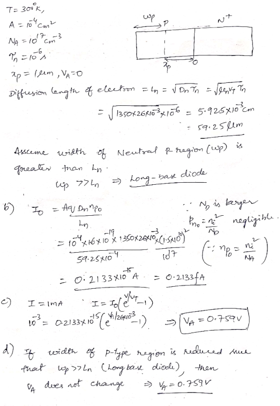
4.15 A PN diode with lengths much larger than the carrier diffusion length such as shown...
 4.15 A PN diode with lengths much larger than the carrier diffusion length such as shown in Fig. 4-18 is called a long-base diode. A short-base diode has lengths much shorter than the diffusion lengths, and its excess carrier concentration is similar to that shown in Fig. 8-6. A uniformly doped short-base Si diode has Nd- 101cm-3and Na 1016cm3. tp n1 us, Dp 10 cms, Dn 30 cm-s, and cross-sectional area10 cm. The length of the quasi-neutral N-type and P-type...
2. (60 pts) Consider a one-sided silicon PN diode. The p-side is degenerately doped (and you...
 2. (60 pts) Consider a one-sided silicon PN diode. The p-side is degenerately doped (and you can assume Ep = Ey for simplicity). The doping concentration on the n-side is Np for 0<x <too. The depletion width on the n-side is xn. Use the depletion approximation. p* ND x 0 From here, you assume that Np is given by 4x1015 cm. (h) (7 pts) What is the maximum electric field in depletion region when Va=-3 V? (i) (8 pts) As...
Wdep P-Type N -Type Q1. Consider the PN junction at equilibrium shown in the figure above....
 Wdep P-Type N -Type Q1. Consider the PN junction at equilibrium shown in the figure above. Both N-side and P-side has same doping density NA ND 1017 /cm3. Assume both electron and hole mobility to be same, i.e Me - 1000cm2/Vs. a equilibrium energy band diagram. Find (EF Et at(i)x-0. (ii) x »xn (iii) X <K_Xp Find the value of built-in voltage and total depletion width (5+5 points) Find electron and hole densities at (i) x = 0. (ii) x...
 this is a problem of semiconductor device and
fundamentals.
Problem 4: pn Junction Current Distributions Consider a Si pn step junction diode maintained at room temperature, with p-side and n-side dopant concentrations NA 1016 cm3 and Np-2x1016 cm3, respectively. (You may assume that each side is uncompensated.) The minority carrier recombination lifetimes are τ,-10-6 s and τ,-10-7 s on the p-side and n-side, respectively a) Calculate the minority carrier densities at the edges of the depletion region when the applied...
this is a problem of semiconductor device and
fundamentals.
Problem 4: pn Junction Current Distributions Consider a Si pn step junction diode maintained at room temperature, with p-side and n-side dopant concentrations NA 1016 cm3 and Np-2x1016 cm3, respectively. (You may assume that each side is uncompensated.) The minority carrier recombination lifetimes are τ,-10-6 s and τ,-10-7 s on the p-side and n-side, respectively a) Calculate the minority carrier densities at the edges of the depletion region when the applied...
 Consider a silicon pn step junction diode with NA-1x1018 cm3 and No 1x1017cm-3, maintained at T 300K. The minority carrier lifetimes in the p-side and n-side are τη-10-8 s and Tp-10-7 s, respectively. a) Calculate the minority carrier densities at the edges of the depletion region when the applied voltage (VA) is 0.6 V. of the junction, for the applied bias voltage of part (a) densities are equal in magnitude, for the applied voltage of part (a). b) Sketch the...
 3.13 Si pn junction Consider a long pn junction diode with an acceptor doping Naof 1018 cm-3 on the p-side and donor concentration of Nj on the n-side. The diode is forward biased and has a voltage of 0.6 V across it. The diode cross-sectional area is 1 mm2. The minority carrier recombination time, T, depends on the total dopant concentration, Ndopant (cm), through the following approximate empirical relation (5x 10⁻⁷)/(1 + 2 10-17N1°pan.) where T is in seconds. (a)...
 3.13 Si pn junction Consider a long pn junction diode with an acceptor doping Naof 1018 cm-3 on the p-side and donor concentration of Nj on the n-side. The diode is forward biased and has a voltage of 0.6 V across it. The diode cross-sectional area is 1 mm2. The minority carrier recombination time, T, depends on the total dopant concentration, Ndopant (cm), through the following approximate empirical relation (5x 10⁻⁷)/(1 + 2 10-17N1°pan.) where T is in seconds. (a)...
 1) Useful parameters for CdTe a. ni- 1e8 cm 3 2) kT 25.8mev Problem #1 (100 points) Consider an ideal, long-diode type solar cell made of a CdTe abrupt asymmetrical PN junction. The relevant properties of the p-type CdTe absorber are: thickness - 3 um, doping - le14 cm3, electron mobility 100 cm2/V/s, and electron lifetime 10 ns. The n type region is doped much higher than CdTe 1. Calculate the saturation current density 2. Calculate the short-circuit current, assuming...
 Problem 3: pn Junction -- Carrier Concentration Profiles The steady-state carrier concentrations inside a Si pn step junction diode maintained at room temperature are shown in the plot below: п or p (log scale Pp -106 10 102 a) Is the diode forward or reverse biased? Explain briefly. b) Do low-level injection conditions prevail in the quasi-neutral regions of the diode? Explain briefly. c) What are the p-side and n-side net dopant concentrations NA and ND, respectively? d) Determine the...
 Assume a p-n step junction in silicon wi concentration of 2x10¹⁶,c? and the n-type material doped at 3X10-s,cm3 The intrinsic carrier density is 1.25X101°/cm and all dopants are fully ionized Assume that the effective density of states for silicon is 3.3x10 cm3 for the conduction band and 1.75x101 cm for the valence band. Assume that the temperature is 300K and silicon relative permittivity of 11.7 a. Compute the hole concentration on the n-side and electron concentration th the p-type material...
 4.15 A PN diode with lengths much larger than the carrier diffusion length such as shown in Fig. 4-18 is called a long-base diode. A short-base diode has lengths much shorter than the diffusion lengths, and its excess carrier concentration is similar to that shown in Fig. 8-6. A uniformly doped short-base Si diode has Nd- 101cm-3and Na 1016cm3. tp n1 us, Dp 10 cms, Dn 30 cm-s, and cross-sectional area10 cm. The length of the quasi-neutral N-type and P-type...
 2. (60 pts) Consider a one-sided silicon PN diode. The p-side is degenerately doped (and you can assume Ep = Ey for simplicity). The doping concentration on the n-side is Np for 0<x <too. The depletion width on the n-side is xn. Use the depletion approximation. p* ND x 0 From here, you assume that Np is given by 4x1015 cm. (h) (7 pts) What is the maximum electric field in depletion region when Va=-3 V? (i) (8 pts) As...
 Wdep P-Type N -Type Q1. Consider the PN junction at equilibrium shown in the figure above. Both N-side and P-side has same doping density NA ND 1017 /cm3. Assume both electron and hole mobility to be same, i.e Me - 1000cm2/Vs. a equilibrium energy band diagram. Find (EF Et at(i)x-0. (ii) x »xn (iii) X <K_Xp Find the value of built-in voltage and total depletion width (5+5 points) Find electron and hole densities at (i) x = 0. (ii) x...
Most questions answered within 3 hours.
-
If a block of Si is doped with 10^17 Boron atom/cm^3 and 5X10^16
Arsenic atoms/cm^3,
(a)...
asked 17 minutes ago -
Why would natural selection not minimize costs (in the form of
symptoms) of evolved defenses? (choose...
asked 35 minutes ago -
What is true about a critical task?
Latest finish time - latest start time = 0...
asked 37 minutes ago -
A company uses a
process costing system. Its Assembly Department's beginning
inventory consisted of 56,800 units,...
asked 37 minutes ago -
a
sealed glass cylinder contains 325 g of N2 gas at 1.02 atm at 20 c....
asked 41 minutes ago -
The main difference between an equity and a nonequity alliance
is that
A
equity alliances are...
asked 40 minutes ago -
Need help with this, in JAVA, using netbeans. A
complete response will receive a positive comment...
asked 48 minutes ago -
An imprest petty cash fund of $600 was established for minor
disbursements. At the end of...
asked 53 minutes ago -
Sharpe Cutter is a small company that produces specialty knives
for paper cutting machinery. The annual...
asked 57 minutes ago -
Calculating the Ka of a weak acid from
pH:
The pH of a 0.68M solution of...
asked 59 minutes ago -
1.What process is pushing back against gravity in the very
center (the core) of sun-like stars?...
asked 1 hour ago -
This question is from the textbook "Python for ArcGIS" by Laura
Tateosian:
Write a script "triangles.py"...
asked 1 hour ago