
Homework Answers
Add Answer to:
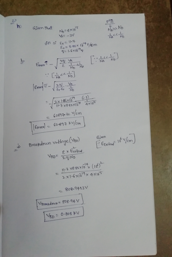
2. (60 pts) Consider a one-sided silicon PN diode. The p-side is degenerately doped (and you...
Q1) A diode has a doping of No- 1019 /cm3 on the n-type side and NA 101/cm3 on the p-type side. W...
 Q1) A diode has a doping of No- 1019 /cm3 on the n-type side and NA 101/cm3 on the p-type side. What are the a) width of depletion region, b) width of depletion region in n side, c) width of depletion region in p side, d) junction potential at zero bias, e) junction width at a reverse bias of 13 V, and f) maximum electric field in zero bias just in the middle of the P-N junction at room temperature?...
A silicon PN junction diode is constructed using N-type silicon in which the Fermi level is...
 A silicon PN junction diode is constructed using N-type silicon in which the Fermi level is 100 meV below the conduction band edge and P-type silicon in which the Fermi level is 120 meV above the valence band edge a) What are the majority and minority carrier concentrations on each side of the junction under thermal equilibrium? b) What is the value of the built-in voltage? c) Determine the width of the depletion region on both sides of the junction...
(iv) [2 Marks] A pn-junction has a built-in potential voltage of 1V across the junction. The width of the depletion reg...
 (iv) [2 Marks] A pn-junction has a built-in potential voltage of 1V across the junction. The width of the depletion region is 1um. The acceptor doping is NA 2 x 1015cm-3 in the P-side and a donor doping is Np = 8 x 1015cm-3 on the N-side. If the reference position x 0 is the edge of the depletion region on the P-side and the P region is on the left of the N region then where does the maximum...
2. Suppose you have a silicon wafer containing a p n junction. Design the doping level on the n-side so that the rev...
 2. Suppose you have a silicon wafer containing a p n junction. Design the doping level on the n-side so that the reverse breakdown voltage is 45 V. and the depletion widths (on the n-side and on the p-side) 3. Calculate the built-in voltage 19 in a silicon pn Junction with Na = 5x101 /cc and Nd = 1 x 10 /cc given that the junction is reverse biased at 5 V. /mi
2. Suppose you have a silicon wafer...
2. Suppose you have a silicon wafer containing a p n junction. Design the doping level on the n-side so that the reverse breakdown voltage is 45 V. and the depletion widths (on the n-side and on the p-side) 3. Calculate the built-in voltage 19 in a silicon pn Junction with Na = 5x101 /cc and Nd = 1 x 10 /cc given that the junction is reverse biased at 5 V. /mi
2. Suppose you have a silicon wafer...
A silicon p+ n step junction diode at room temperature has N_d = 10^16 cm-3. a)...
A silicon p+ n step junction diode at room temperature has N_d = 10^16 cm-3. a) What breakdown mechanism do you expect will be dominant in this device? Explain. b) Find the approximate breakdown voltage for this diode. c) Calculate the depletion width at the breakdown voltage. d) What is the maximum magnitude of the electric field in the depletion region at the breakdown voltage?
THE REVERSE BIAS VOLTAGE APPLIED TO SILICON PN JUNCTION DIODE IS 4V, DOPING CONCENTRATION Na is...
THE REVERSE BIAS VOLTAGE APPLIED TO SILICON PN JUNCTION DIODE IS 4V, DOPING CONCENTRATION Na is 10^17 cm^-3, Nd = 10^16 cm^-3, ni = 1.3 x 10^9 cm^-3, temperature T = 273 k find the width of depletion region with the applied reverse voltage please check your answer that it is correct please it is a humble request
Design an ideal abrupt silicon PN-junction at 300 K such that the donor impurity concentration in...
 XXX is 467
Design an ideal abrupt silicon PN-junction at 300 K such that the donor impurity concentration in the n-side N, = 5x1015 cm3 and the acceptor impurity concentration in the p-side N, = XXX × 1015/cm3 Assume that the diode area A-2x10⁻³ cm2 and 100cm work Note that the values obtained in the calculations may not be realistic as the Matric # varies greatly. The assignment is only to test your understanding, and must be handwritten Determine the...
XXX is 467
Design an ideal abrupt silicon PN-junction at 300 K such that the donor impurity concentration in the n-side N, = 5x1015 cm3 and the acceptor impurity concentration in the p-side N, = XXX × 1015/cm3 Assume that the diode area A-2x10⁻³ cm2 and 100cm work Note that the values obtained in the calculations may not be realistic as the Matric # varies greatly. The assignment is only to test your understanding, and must be handwritten Determine the...
1.You have a piece of intrinsic silicon. explain how to convert it to n-type. 2.The depletion...
1.You have a piece of intrinsic silicon. explain how to convert it to n-type. 2.The depletion region is a region in the pn junction that is depleted from................. 3.Decreasing the amount of doping to an intrinsic semiconductor, causes the resistance of the doped silicon to................ 4.What is a p-type semiconductor? 5.As the amount of doping to an intrinsic semiconductor increases, the resistance of the doped silicon................
Problem 4: Narrow-Base Diode Consider an ideal pn* step-junction Si diode maintained at 300K with cross-sectional...
 Problem 4: Narrow-Base Diode Consider an ideal pn* step-junction Si diode maintained at 300K with cross-sectional area A = 104cm2. The doping concentration on the p-type side is Na= 1017 cm3 (uncompensated). (The n-type side is degenerately doped.) The electron recombination lifetime in the p-type region is tn = 10-6 s. The width of the quasi-neutral p-type region is 1 um, for VA=0 V. a Is this a narrow-base diode? Justify your answer. b) Calculate the diode saturation current Io....
Assume a p-n step junction in silicon wi concentration of 2x10¹⁶,c? and the n-type material doped...
 Assume a p-n step junction in silicon wi concentration of 2x10¹⁶,c? and the n-type material doped at 3X10-s,cm3 The intrinsic carrier density is 1.25X101°/cm and all dopants are fully ionized Assume that the effective density of states for silicon is 3.3x10 cm3 for the conduction band and 1.75x101 cm for the valence band. Assume that the temperature is 300K and silicon relative permittivity of 11.7 a. Compute the hole concentration on the n-side and electron concentration th the p-type material...
 Q1) A diode has a doping of No- 1019 /cm3 on the n-type side and NA 101/cm3 on the p-type side. What are the a) width of depletion region, b) width of depletion region in n side, c) width of depletion region in p side, d) junction potential at zero bias, e) junction width at a reverse bias of 13 V, and f) maximum electric field in zero bias just in the middle of the P-N junction at room temperature?...
 A silicon PN junction diode is constructed using N-type silicon in which the Fermi level is 100 meV below the conduction band edge and P-type silicon in which the Fermi level is 120 meV above the valence band edge a) What are the majority and minority carrier concentrations on each side of the junction under thermal equilibrium? b) What is the value of the built-in voltage? c) Determine the width of the depletion region on both sides of the junction...
 (iv) [2 Marks] A pn-junction has a built-in potential voltage of 1V across the junction. The width of the depletion region is 1um. The acceptor doping is NA 2 x 1015cm-3 in the P-side and a donor doping is Np = 8 x 1015cm-3 on the N-side. If the reference position x 0 is the edge of the depletion region on the P-side and the P region is on the left of the N region then where does the maximum...
 2. Suppose you have a silicon wafer containing a p n junction. Design the doping level on the n-side so that the reverse breakdown voltage is 45 V. and the depletion widths (on the n-side and on the p-side) 3. Calculate the built-in voltage 19 in a silicon pn Junction with Na = 5x101 /cc and Nd = 1 x 10 /cc given that the junction is reverse biased at 5 V. /mi
2. Suppose you have a silicon wafer...
2. Suppose you have a silicon wafer containing a p n junction. Design the doping level on the n-side so that the reverse breakdown voltage is 45 V. and the depletion widths (on the n-side and on the p-side) 3. Calculate the built-in voltage 19 in a silicon pn Junction with Na = 5x101 /cc and Nd = 1 x 10 /cc given that the junction is reverse biased at 5 V. /mi
2. Suppose you have a silicon wafer...
 XXX is 467
Design an ideal abrupt silicon PN-junction at 300 K such that the donor impurity concentration in the n-side N, = 5x1015 cm3 and the acceptor impurity concentration in the p-side N, = XXX × 1015/cm3 Assume that the diode area A-2x10⁻³ cm2 and 100cm work Note that the values obtained in the calculations may not be realistic as the Matric # varies greatly. The assignment is only to test your understanding, and must be handwritten Determine the...
XXX is 467
Design an ideal abrupt silicon PN-junction at 300 K such that the donor impurity concentration in the n-side N, = 5x1015 cm3 and the acceptor impurity concentration in the p-side N, = XXX × 1015/cm3 Assume that the diode area A-2x10⁻³ cm2 and 100cm work Note that the values obtained in the calculations may not be realistic as the Matric # varies greatly. The assignment is only to test your understanding, and must be handwritten Determine the...
 Problem 4: Narrow-Base Diode Consider an ideal pn* step-junction Si diode maintained at 300K with cross-sectional area A = 104cm2. The doping concentration on the p-type side is Na= 1017 cm3 (uncompensated). (The n-type side is degenerately doped.) The electron recombination lifetime in the p-type region is tn = 10-6 s. The width of the quasi-neutral p-type region is 1 um, for VA=0 V. a Is this a narrow-base diode? Justify your answer. b) Calculate the diode saturation current Io....
 Assume a p-n step junction in silicon wi concentration of 2x10¹⁶,c? and the n-type material doped at 3X10-s,cm3 The intrinsic carrier density is 1.25X101°/cm and all dopants are fully ionized Assume that the effective density of states for silicon is 3.3x10 cm3 for the conduction band and 1.75x101 cm for the valence band. Assume that the temperature is 300K and silicon relative permittivity of 11.7 a. Compute the hole concentration on the n-side and electron concentration th the p-type material...
Most questions answered within 3 hours.
-
Write an essay containing your thoughts on
whether corporations should be limited in the amount of...
asked 6 minutes ago -
A 4.0 L flask containing chlorine gas is connected to an
evacuated 3.0 L flask. If...
asked 6 minutes ago -
Given the following two sequences x (n)=[3 , 11,7 ,0 ,−1, 4 ,2
],−3≤n≤ 3 ;...
asked 6 minutes ago -
What is the minimal sample size needed for a 95% confidence
interval to have a maximal...
asked 7 minutes ago -
1. Methods of collecting data - Experiments and direct
observation
In each of the following situations,...
asked 21 minutes ago -
Each protein is composed of a maximum of ____________ different
amino acids in varying numbers and...
asked 38 minutes ago -
One member in the comp set that did not have supply, demand, and
revenue data. What...
asked 16 minutes ago -
What is the density of a substance that takes up 3.4e3 cubic cm
and weighs 1.96...
asked 31 minutes ago -
Consider a single wire loop of radius a. Calculate the magnetic
field B(z) along the axis...
asked 27 minutes ago -
For each of the compounds listed below you must draw the Lewis
dot structure in the...
asked 30 minutes ago -
1. Hypothesize in what type of environments it would be
advantageous for a protist to be...
asked 29 minutes ago -
The mayor of a town has proposed a plan for the construction of
a new community....
asked 48 minutes ago