
Homework Answers


Add Answer to:
3.13 Si pn junction Consider a long pn junction diode with an acceptor doping Naof 1018...
3.13 Si pn junction Consider a long pn junction diode with an acceptor doping Naof 1018 cm-3 on t...
 3.13 Si pn junction Consider a long pn junction diode with an acceptor doping Naof 1018 cm-3 on the p-side and donor concentration of Nj on the n-side. The diode is forward biased and has a voltage of 0.6 V across it. The diode cross-sectional area is 1 mm2. The minority carrier recombination time, T, depends on the total dopant concentration, Ndopant (cm), through the following approximate empirical relation (5x 10⁻⁷)/(1 + 2 10-17N1°pan.) where T is in seconds. (a)...
Problem 3: pn Junction -- Carrier Concentration Profiles The steady-state carrier concentrations inside a Si pn step ju...
 Problem 3: pn Junction -- Carrier Concentration Profiles The steady-state carrier concentrations inside a Si pn step junction diode maintained at room temperature are shown in the plot below: п or p (log scale Pp -106 10 102 a) Is the diode forward or reverse biased? Explain briefly. b) Do low-level injection conditions prevail in the quasi-neutral regions of the diode? Explain briefly. c) What are the p-side and n-side net dopant concentrations NA and ND, respectively? d) Determine the...
this is a problem of semiconductor device and fundamentals. Problem 4: pn Junction Current Distributions Consider a...
 this is a problem of semiconductor device and
fundamentals.
Problem 4: pn Junction Current Distributions Consider a Si pn step junction diode maintained at room temperature, with p-side and n-side dopant concentrations NA 1016 cm3 and Np-2x1016 cm3, respectively. (You may assume that each side is uncompensated.) The minority carrier recombination lifetimes are τ,-10-6 s and τ,-10-7 s on the p-side and n-side, respectively a) Calculate the minority carrier densities at the edges of the depletion region when the applied...
this is a problem of semiconductor device and
fundamentals.
Problem 4: pn Junction Current Distributions Consider a Si pn step junction diode maintained at room temperature, with p-side and n-side dopant concentrations NA 1016 cm3 and Np-2x1016 cm3, respectively. (You may assume that each side is uncompensated.) The minority carrier recombination lifetimes are τ,-10-6 s and τ,-10-7 s on the p-side and n-side, respectively a) Calculate the minority carrier densities at the edges of the depletion region when the applied...
3. An ideal Si pn junction at 300 K is under forward bias. The minority carrier...
 3. An ideal Si pn junction at 300 K is under forward bias. The minority carrier life times are 10* and 107 s for electrons and holes. The doping concentration in the n-region is ND-10° cmPlot the ratio of hole current to the total current crossing the space charge region as the p-region doping concentration (NA varies over the range 1014 to 1018 cnm Use a log scale for the doping concentrations.[use Fig.3.5(a) on P80 for mobility values) 163 cm....
Design an ideal abrupt silicon PN-junction at 300 K such that the donor impurity concentration in...
 XXX is 467
Design an ideal abrupt silicon PN-junction at 300 K such that the donor impurity concentration in the n-side N, = 5x1015 cm3 and the acceptor impurity concentration in the p-side N, = XXX × 1015/cm3 Assume that the diode area A-2x10⁻³ cm2 and 100cm work Note that the values obtained in the calculations may not be realistic as the Matric # varies greatly. The assignment is only to test your understanding, and must be handwritten Determine the...
XXX is 467
Design an ideal abrupt silicon PN-junction at 300 K such that the donor impurity concentration in the n-side N, = 5x1015 cm3 and the acceptor impurity concentration in the p-side N, = XXX × 1015/cm3 Assume that the diode area A-2x10⁻³ cm2 and 100cm work Note that the values obtained in the calculations may not be realistic as the Matric # varies greatly. The assignment is only to test your understanding, and must be handwritten Determine the...
Problem 4: Narrow-Base Diode Consider an ideal pn* step-junction Si diode maintained at 300K with cross-sectional...
 Problem 4: Narrow-Base Diode Consider an ideal pn* step-junction Si diode maintained at 300K with cross-sectional area A = 104cm2. The doping concentration on the p-type side is Na= 1017 cm3 (uncompensated). (The n-type side is degenerately doped.) The electron recombination lifetime in the p-type region is tn = 10-6 s. The width of the quasi-neutral p-type region is 1 um, for VA=0 V. a Is this a narrow-base diode? Justify your answer. b) Calculate the diode saturation current Io....
A pn junction diode is made of a new semiconductor with 10^16cm-3 acceptors in the p...
A pn junction diode is made of a new semiconductor with 10^16cm-3 acceptors in the p side and 2x10^17cm-3 donors on the n-side. Intrinsic carrier concentration is same as silicon 10^10cm-3 at room temperature. Let's assume that a forward bias voltage is applied in a way that it create following minority carrier concentrations in quasi neutral regions. n(x) =10^4 - 10^14/[10^4(x+xp)-1] (cm-3) where x<xp<0 and p(x) = 500+10^15/[10^4(x+xn)+1] (cm-3) where x>xn>0. x is given in cm scale. Calculate the total...
A pn junction diode is made of a new semiconductor with 10^16cm-3 donors in the n...
A pn junction diode is made of a new semiconductor with 10^16cm-3 donors in the n side and 2x10^17cm-3 acceptors on the p-side. Intrinsic carrier concentration is same as silicon 10^10cm-3at room temperature. Let's assume that a forward bias voltage is applied in a way that it create following minority carrier concentrations in quasi neutral regions. p(x) =10^4 + 10^14/[1+10^4(x-xn)] (cm-3) where x>xn>0 and n(x) = 500-10^15/[10^4(x+xp)-1] (cm-3) where x<-xp<0. x is given in cm scale. Calculate the total current...
Q3 Consider a GaAs pn junction with doping concentrations Na5 x 106 cm-3 and N1016 cm-3....
 Q3 Consider a GaAs pn junction with doping concentrations Na5 x 106 cm-3 and N1016 cm-3. The junction cross-sectional area is A 103 cm2 and the applied forward-bias voltage is Va 1.10 V. Calculate the (a) minority electron diffusion cur rent at the edge of the space charge region, (b) minority hole diffusion current at the edge of the space charge region, and (c) total current in the pn junction diode.
1o points: Conside r an abrupt Si pn junction that has 10 acceptors em3 on the p-side donors on t...
 asap. please
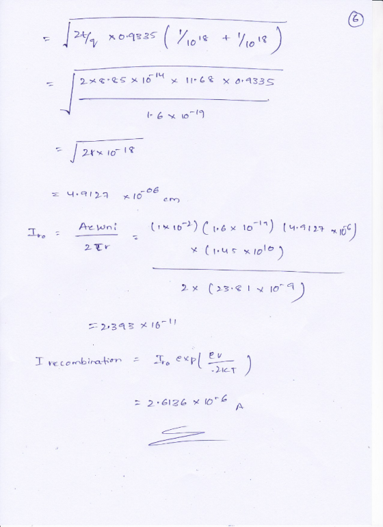
1o points: Conside r an abrupt Si pn junction that has 10 acceptors em3 on the p-side donors on the n-side. The minority carier recombination times are fe-490 ns for and 109 electrons in the 1350 cm Vs, and with Nd-10 cm and A,s 65 cm ,The cross-sectional area is 1.5 mm. Assume this is a long diode, please calculate the current, I, hrough the diode at room temperature when the voltage, V, acoss it is 0.25 2.5...
asap. please
1o points: Conside r an abrupt Si pn junction that has 10 acceptors em3 on the p-side donors on the n-side. The minority carier recombination times are fe-490 ns for and 109 electrons in the 1350 cm Vs, and with Nd-10 cm and A,s 65 cm ,The cross-sectional area is 1.5 mm. Assume this is a long diode, please calculate the current, I, hrough the diode at room temperature when the voltage, V, acoss it is 0.25 2.5...
 3.13 Si pn junction Consider a long pn junction diode with an acceptor doping Naof 1018 cm-3 on the p-side and donor concentration of Nj on the n-side. The diode is forward biased and has a voltage of 0.6 V across it. The diode cross-sectional area is 1 mm2. The minority carrier recombination time, T, depends on the total dopant concentration, Ndopant (cm), through the following approximate empirical relation (5x 10⁻⁷)/(1 + 2 10-17N1°pan.) where T is in seconds. (a)...
 Problem 3: pn Junction -- Carrier Concentration Profiles The steady-state carrier concentrations inside a Si pn step junction diode maintained at room temperature are shown in the plot below: п or p (log scale Pp -106 10 102 a) Is the diode forward or reverse biased? Explain briefly. b) Do low-level injection conditions prevail in the quasi-neutral regions of the diode? Explain briefly. c) What are the p-side and n-side net dopant concentrations NA and ND, respectively? d) Determine the...
 this is a problem of semiconductor device and
fundamentals.
Problem 4: pn Junction Current Distributions Consider a Si pn step junction diode maintained at room temperature, with p-side and n-side dopant concentrations NA 1016 cm3 and Np-2x1016 cm3, respectively. (You may assume that each side is uncompensated.) The minority carrier recombination lifetimes are τ,-10-6 s and τ,-10-7 s on the p-side and n-side, respectively a) Calculate the minority carrier densities at the edges of the depletion region when the applied...
this is a problem of semiconductor device and
fundamentals.
Problem 4: pn Junction Current Distributions Consider a Si pn step junction diode maintained at room temperature, with p-side and n-side dopant concentrations NA 1016 cm3 and Np-2x1016 cm3, respectively. (You may assume that each side is uncompensated.) The minority carrier recombination lifetimes are τ,-10-6 s and τ,-10-7 s on the p-side and n-side, respectively a) Calculate the minority carrier densities at the edges of the depletion region when the applied...
 3. An ideal Si pn junction at 300 K is under forward bias. The minority carrier life times are 10* and 107 s for electrons and holes. The doping concentration in the n-region is ND-10° cmPlot the ratio of hole current to the total current crossing the space charge region as the p-region doping concentration (NA varies over the range 1014 to 1018 cnm Use a log scale for the doping concentrations.[use Fig.3.5(a) on P80 for mobility values) 163 cm....
 XXX is 467
Design an ideal abrupt silicon PN-junction at 300 K such that the donor impurity concentration in the n-side N, = 5x1015 cm3 and the acceptor impurity concentration in the p-side N, = XXX × 1015/cm3 Assume that the diode area A-2x10⁻³ cm2 and 100cm work Note that the values obtained in the calculations may not be realistic as the Matric # varies greatly. The assignment is only to test your understanding, and must be handwritten Determine the...
XXX is 467
Design an ideal abrupt silicon PN-junction at 300 K such that the donor impurity concentration in the n-side N, = 5x1015 cm3 and the acceptor impurity concentration in the p-side N, = XXX × 1015/cm3 Assume that the diode area A-2x10⁻³ cm2 and 100cm work Note that the values obtained in the calculations may not be realistic as the Matric # varies greatly. The assignment is only to test your understanding, and must be handwritten Determine the...
 Problem 4: Narrow-Base Diode Consider an ideal pn* step-junction Si diode maintained at 300K with cross-sectional area A = 104cm2. The doping concentration on the p-type side is Na= 1017 cm3 (uncompensated). (The n-type side is degenerately doped.) The electron recombination lifetime in the p-type region is tn = 10-6 s. The width of the quasi-neutral p-type region is 1 um, for VA=0 V. a Is this a narrow-base diode? Justify your answer. b) Calculate the diode saturation current Io....
 Q3 Consider a GaAs pn junction with doping concentrations Na5 x 106 cm-3 and N1016 cm-3. The junction cross-sectional area is A 103 cm2 and the applied forward-bias voltage is Va 1.10 V. Calculate the (a) minority electron diffusion cur rent at the edge of the space charge region, (b) minority hole diffusion current at the edge of the space charge region, and (c) total current in the pn junction diode.
 asap. please
1o points: Conside r an abrupt Si pn junction that has 10 acceptors em3 on the p-side donors on the n-side. The minority carier recombination times are fe-490 ns for and 109 electrons in the 1350 cm Vs, and with Nd-10 cm and A,s 65 cm ,The cross-sectional area is 1.5 mm. Assume this is a long diode, please calculate the current, I, hrough the diode at room temperature when the voltage, V, acoss it is 0.25 2.5...
asap. please
1o points: Conside r an abrupt Si pn junction that has 10 acceptors em3 on the p-side donors on the n-side. The minority carier recombination times are fe-490 ns for and 109 electrons in the 1350 cm Vs, and with Nd-10 cm and A,s 65 cm ,The cross-sectional area is 1.5 mm. Assume this is a long diode, please calculate the current, I, hrough the diode at room temperature when the voltage, V, acoss it is 0.25 2.5...
Most questions answered within 3 hours.
-
Write a program to solve the Josephus problem, with the following
modification:
Sample Input:
./a.out n...
asked 2 hours ago -
At the start of a CD it is spinning at a rate of 525 rpm
(revolutions...
asked 3 hours ago -
4. Without doing any calculations, predict whether the observed
∆T would increase, decrease or remain the...
asked 4 hours ago -
Based on the range, which of the following sets of scores has
the greatest variability? 3,...
asked 5 hours ago -
Ripples in a pond travel at a velocity of 3 m/s with one peak
passing a...
asked 5 hours ago -
A man stands on the roof of a building of height 13.0 mm and
throws a...
asked 5 hours ago -
The extent to which assets are financed by borrowed funds and
other liabilities is indicated by:...
asked 6 hours ago -
Explain in detail
Germany is the fifth largest economy
explain what goods and services Germany specializes...
asked 6 hours ago -
The density of platinum is 21.45 g/mL. If a cube of platinum
with a mass of...
asked 6 hours ago -
Accounts Receivable
Sales
A/R Posting
Extended Sales Invoice
Packing Slip
Compare invoice to packing slip 2...
asked 6 hours ago -
Michaella, age 23, is a full-time law student and is claimed by
her parents as a...
asked 6 hours ago -
Why are polymers not typically casted into products?
asked 7 hours ago