
Homework Answers


Add Answer to:
*5. Design a BJT transistor drive circuit like the one shown Figure 10-7 (Hart's text) with an in...
*5. Design a BJT transistor drive circuit like the one shown Figure 10-7 (Hart's text) with...
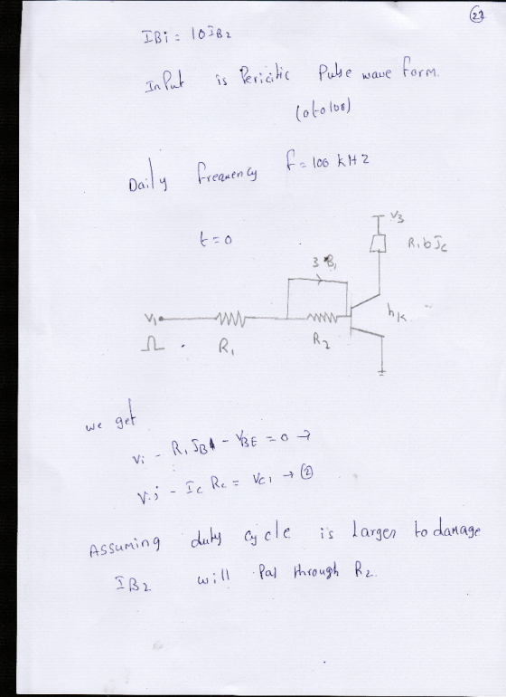
 *5. Design a BJT transistor drive circuit like the one shown Figure 10-7 (Hart's text) with an initial peak base current, IB,-8 1B2, where 1B2 denotes the minimum base current required to drive the transistor to saturation. Assume a collector load resistance, Rc-8 Ω, collector supply voltage Vs = 30 V, large signal current of the transistor, hFE-min. 10, max. 20), VBE(on)-0.8 V, and the input is periodic pulse waveform (0 to 6) V, with a duty cycle, D-0.5. Also,...
The NPN transistor in the circuit shown haes B-60 Assuming that the BJT is operating in the deep ...
 answer i-iv please
The NPN transistor in the circuit shown haes B-60 Assuming that the BJT is operating in the deep saturation mode ie. VCEsat-02y and VBE-07V ßforced-10. Question 3: 20% p-60) Assuming that the BJT is operating in the deep Rg i) Calculate collector current, Ic. (4%) ii) Calculate voltage VBB and base current,IB(6%) iii) If we keep VBB and Rc the same, i.e. at 1k2, what is the minimum value of RB to restore the transistor beta to...
answer i-iv please
The NPN transistor in the circuit shown haes B-60 Assuming that the BJT is operating in the deep saturation mode ie. VCEsat-02y and VBE-07V ßforced-10. Question 3: 20% p-60) Assuming that the BJT is operating in the deep Rg i) Calculate collector current, Ic. (4%) ii) Calculate voltage VBB and base current,IB(6%) iii) If we keep VBB and Rc the same, i.e. at 1k2, what is the minimum value of RB to restore the transistor beta to...
D. For the transistor circuit shown in Figure 7, assuming that the transistor is in the...
 D. For the transistor circuit shown in Figure 7, assuming that the transistor is in the forward active mode, and B = 100 and VBE = 0.7V, calculate Base current 1B Collector current Ic (iii) Emitter current le (iv) Collector to emitter voltage Vce and (v) Voltage across the 2009 resistor v 3 80022 10 kV W VCE VBE مت + + 1 2001} 1 1
draw a base biased circuit and refered to question 5 and complete table. please draw the fixed bias diagram circuit and follow throught step on the next question. Figure 1. Bipolar junction tran...
 draw a base biased circuit and refered to question 5 and
complete table.
please draw the fixed bias diagram circuit and follow throught step
on the next question.
Figure 1. Bipolar junction transistor under base bias/fixed bias 5. In the circuit drawn in Figure 1, label the components with the following values: Base voltage, Collector voltage10V Base resistance Collector resistance Base - emitter voltage 2.7 k2 0.7 V 160 6. Connect the circuit drawn in Figure 1 on the breadboard....
draw a base biased circuit and refered to question 5 and
complete table.
please draw the fixed bias diagram circuit and follow throught step
on the next question.
Figure 1. Bipolar junction transistor under base bias/fixed bias 5. In the circuit drawn in Figure 1, label the components with the following values: Base voltage, Collector voltage10V Base resistance Collector resistance Base - emitter voltage 2.7 k2 0.7 V 160 6. Connect the circuit drawn in Figure 1 on the breadboard....
Figure 3 Transistor amplifire circuit with source Vs and load R b) For the BJT switching...
 Figure 3 Transistor amplifire circuit with source Vs and load R b) For the BJT switching circuit shown in Figure 4, i) Calculate the value of Ra so that the transistor is operating in saturation when switched on if the value of Rc is 3.9 kn. ii) What will the output voltage be for the applied input signal voltage shown if Vcet IS 0.2V? 5 V Re o V 5 V B 100 OV Figure 4 BUT switching circuit with...
4. Lab VIII: Experiment VII The Bipolar Junction Transistor (BJT) Characteristics The bipolar junction transistor (BJT)...
 4. Lab VIII: Experiment VII The Bipolar Junction Transistor (BJT) Characteristics The bipolar junction transistor (BJT) is a three-terminal solid state device widely used as an amplifier (or switching) device. It consists of two n-type materials sandwiched by p-type material (npn) or two p-type and n-type. The terminals (sections) are known as emitter E, base B and collector C. Two currents and two voltages uniquely describe the behavior of the device. The third current/voltage can be determined through KCL/KVL. See...
ASAP! Question 1 [Soalan 1] (a) Describe the condition when a npn BJT transistor operates in...
 ASAP!
Question 1 [Soalan 1] (a) Describe the condition when a npn BJT transistor operates in saturation condition and what are the terminal currents and voltages conditions during saturation. [Terangkan keadaan bila satu transistor BJT npn beroperasi dalam keadaan tepu dan apakah keadaan arus dan voltan terminal semasa tepu. ] (20 Marks/Markah) (b) Consider the BJT transistor circuit in Figure 1. If Bpc = 100 and VBE = 0.65V, calculate: [Pertimbangkan litar transistor BJT dalam Rajah 1. Jika Bpc =...
ASAP!
Question 1 [Soalan 1] (a) Describe the condition when a npn BJT transistor operates in saturation condition and what are the terminal currents and voltages conditions during saturation. [Terangkan keadaan bila satu transistor BJT npn beroperasi dalam keadaan tepu dan apakah keadaan arus dan voltan terminal semasa tepu. ] (20 Marks/Markah) (b) Consider the BJT transistor circuit in Figure 1. If Bpc = 100 and VBE = 0.65V, calculate: [Pertimbangkan litar transistor BJT dalam Rajah 1. Jika Bpc =...
2. a) Suppose the input to the following BJT switching cri is perd and duty cycle,...
 2. a) Suppose the input to the following BJT switching cri is perd and duty cycle, D, varies between 0.2 and 0.5. Also, assume that the circuit is operating rectangeil i tngiw in steady state snl The switch needs to be designed such that the BJT is driven to saturation in the worst case scenario. First alent circuit model when the switch is closed and determine the maximum collector ( max. Then use the information provided in the following Table...
IX With reference to the transistor amplifier shown in Figure QB4 below d For the bipolar transistor circuit of Figure QB4 the following DC bias conditions were measured: VB made. 1.6 V and VBE =0.6...
 IX With reference to the transistor amplifier shown in Figure QB4 below d For the bipolar transistor circuit of Figure QB4 the following DC bias conditions were measured: VB made. 1.6 V and VBE =0.6 V. Detemine the value for RA, stating any assumptions e) Using these same conditions, calculate the current in Re and deduce the current in Rc, stating any assumptions made. Hence find the voltage across Rc and explain whether this voltage is suitable for this amplifier...
Could someone please help me on how I should be configuring the circuit in Figure 4(a)...
 Could someone please help me on how I should be configuring the
circuit in Figure 4(a) in Multisim? Basically not understanding
question #1 in the Procedure. Cannot keep Vrb the same value while
adjusting Vcc. Then when trying to adjust Vbb to hold Vrb, Ib
changes.
Any help is appreciated!
Discrete Devices Section LAB 4 BJT CHARACTERISTICS AND BIASING Objective: The objective of this laboratory is to examine the operation of a bipolar junction transistor and plot its output characteristics...
Could someone please help me on how I should be configuring the
circuit in Figure 4(a) in Multisim? Basically not understanding
question #1 in the Procedure. Cannot keep Vrb the same value while
adjusting Vcc. Then when trying to adjust Vbb to hold Vrb, Ib
changes.
Any help is appreciated!
Discrete Devices Section LAB 4 BJT CHARACTERISTICS AND BIASING Objective: The objective of this laboratory is to examine the operation of a bipolar junction transistor and plot its output characteristics...
 *5. Design a BJT transistor drive circuit like the one shown Figure 10-7 (Hart's text) with an initial peak base current, IB,-8 1B2, where 1B2 denotes the minimum base current required to drive the transistor to saturation. Assume a collector load resistance, Rc-8 Ω, collector supply voltage Vs = 30 V, large signal current of the transistor, hFE-min. 10, max. 20), VBE(on)-0.8 V, and the input is periodic pulse waveform (0 to 6) V, with a duty cycle, D-0.5. Also,...
 answer i-iv please
The NPN transistor in the circuit shown haes B-60 Assuming that the BJT is operating in the deep saturation mode ie. VCEsat-02y and VBE-07V ßforced-10. Question 3: 20% p-60) Assuming that the BJT is operating in the deep Rg i) Calculate collector current, Ic. (4%) ii) Calculate voltage VBB and base current,IB(6%) iii) If we keep VBB and Rc the same, i.e. at 1k2, what is the minimum value of RB to restore the transistor beta to...
answer i-iv please
The NPN transistor in the circuit shown haes B-60 Assuming that the BJT is operating in the deep saturation mode ie. VCEsat-02y and VBE-07V ßforced-10. Question 3: 20% p-60) Assuming that the BJT is operating in the deep Rg i) Calculate collector current, Ic. (4%) ii) Calculate voltage VBB and base current,IB(6%) iii) If we keep VBB and Rc the same, i.e. at 1k2, what is the minimum value of RB to restore the transistor beta to...
 D. For the transistor circuit shown in Figure 7, assuming that the transistor is in the forward active mode, and B = 100 and VBE = 0.7V, calculate Base current 1B Collector current Ic (iii) Emitter current le (iv) Collector to emitter voltage Vce and (v) Voltage across the 2009 resistor v 3 80022 10 kV W VCE VBE مت + + 1 2001} 1 1
 draw a base biased circuit and refered to question 5 and
complete table.
please draw the fixed bias diagram circuit and follow throught step
on the next question.
Figure 1. Bipolar junction transistor under base bias/fixed bias 5. In the circuit drawn in Figure 1, label the components with the following values: Base voltage, Collector voltage10V Base resistance Collector resistance Base - emitter voltage 2.7 k2 0.7 V 160 6. Connect the circuit drawn in Figure 1 on the breadboard....
draw a base biased circuit and refered to question 5 and
complete table.
please draw the fixed bias diagram circuit and follow throught step
on the next question.
Figure 1. Bipolar junction transistor under base bias/fixed bias 5. In the circuit drawn in Figure 1, label the components with the following values: Base voltage, Collector voltage10V Base resistance Collector resistance Base - emitter voltage 2.7 k2 0.7 V 160 6. Connect the circuit drawn in Figure 1 on the breadboard....
 Figure 3 Transistor amplifire circuit with source Vs and load R b) For the BJT switching circuit shown in Figure 4, i) Calculate the value of Ra so that the transistor is operating in saturation when switched on if the value of Rc is 3.9 kn. ii) What will the output voltage be for the applied input signal voltage shown if Vcet IS 0.2V? 5 V Re o V 5 V B 100 OV Figure 4 BUT switching circuit with...
 4. Lab VIII: Experiment VII The Bipolar Junction Transistor (BJT) Characteristics The bipolar junction transistor (BJT) is a three-terminal solid state device widely used as an amplifier (or switching) device. It consists of two n-type materials sandwiched by p-type material (npn) or two p-type and n-type. The terminals (sections) are known as emitter E, base B and collector C. Two currents and two voltages uniquely describe the behavior of the device. The third current/voltage can be determined through KCL/KVL. See...
 ASAP!
Question 1 [Soalan 1] (a) Describe the condition when a npn BJT transistor operates in saturation condition and what are the terminal currents and voltages conditions during saturation. [Terangkan keadaan bila satu transistor BJT npn beroperasi dalam keadaan tepu dan apakah keadaan arus dan voltan terminal semasa tepu. ] (20 Marks/Markah) (b) Consider the BJT transistor circuit in Figure 1. If Bpc = 100 and VBE = 0.65V, calculate: [Pertimbangkan litar transistor BJT dalam Rajah 1. Jika Bpc =...
ASAP!
Question 1 [Soalan 1] (a) Describe the condition when a npn BJT transistor operates in saturation condition and what are the terminal currents and voltages conditions during saturation. [Terangkan keadaan bila satu transistor BJT npn beroperasi dalam keadaan tepu dan apakah keadaan arus dan voltan terminal semasa tepu. ] (20 Marks/Markah) (b) Consider the BJT transistor circuit in Figure 1. If Bpc = 100 and VBE = 0.65V, calculate: [Pertimbangkan litar transistor BJT dalam Rajah 1. Jika Bpc =...
 2. a) Suppose the input to the following BJT switching cri is perd and duty cycle, D, varies between 0.2 and 0.5. Also, assume that the circuit is operating rectangeil i tngiw in steady state snl The switch needs to be designed such that the BJT is driven to saturation in the worst case scenario. First alent circuit model when the switch is closed and determine the maximum collector ( max. Then use the information provided in the following Table...
 IX With reference to the transistor amplifier shown in Figure QB4 below d For the bipolar transistor circuit of Figure QB4 the following DC bias conditions were measured: VB made. 1.6 V and VBE =0.6 V. Detemine the value for RA, stating any assumptions e) Using these same conditions, calculate the current in Re and deduce the current in Rc, stating any assumptions made. Hence find the voltage across Rc and explain whether this voltage is suitable for this amplifier...
 Could someone please help me on how I should be configuring the
circuit in Figure 4(a) in Multisim? Basically not understanding
question #1 in the Procedure. Cannot keep Vrb the same value while
adjusting Vcc. Then when trying to adjust Vbb to hold Vrb, Ib
changes.
Any help is appreciated!
Discrete Devices Section LAB 4 BJT CHARACTERISTICS AND BIASING Objective: The objective of this laboratory is to examine the operation of a bipolar junction transistor and plot its output characteristics...
Could someone please help me on how I should be configuring the
circuit in Figure 4(a) in Multisim? Basically not understanding
question #1 in the Procedure. Cannot keep Vrb the same value while
adjusting Vcc. Then when trying to adjust Vbb to hold Vrb, Ib
changes.
Any help is appreciated!
Discrete Devices Section LAB 4 BJT CHARACTERISTICS AND BIASING Objective: The objective of this laboratory is to examine the operation of a bipolar junction transistor and plot its output characteristics...
Most questions answered within 3 hours.
-
What specific indicators can point to lack of progress for
African Americans in American society?
asked 4 minutes ago -
1-The Electrons in a beam are moving at 2.7×10⁸ m/s in an
electric field of 15000...
asked 20 minutes ago -
A gas tank is a vertical cylinder. It has a radius of 1m, a
height of...
asked 46 minutes ago -
Accent Software faces the following conditions. All of these
support Accent’s use of a market-penetration pricing...
asked 1 hour ago -
A mathematically inclined friend emails you the following
instructions: "Meet me in the cafeteria the first...
asked 1 hour ago -
A monopoly sells in two countries . The demand curves in the two
countries are p1...
asked 2 hours ago -
A .15kg rubber ball is bounced off a wall. Before hitting the
wall, the ball moves...
asked 3 hours ago -
A manufacturing company preparing to build a new plant is
considering three potential locations for it....
asked 3 hours ago -
B. If compound Y has approximately the same values of solubility
in toluene as compound X,...
asked 4 hours ago -
Oscar Inc. has inventory in Japan valued at 39,051,000 Yen one
year ago. One year ago...
asked 4 hours ago -
If Canada suffered from "fundamental disequilibrium," and its
government choose not to devalue its currency, a...
asked 4 hours ago -
4. How many input & output Key Value Pairs are passed into,
and emitted out of...
asked 4 hours ago