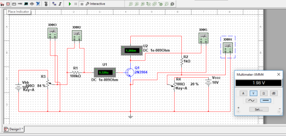
Could someone please help me on how I should be configuring the circuit in Figure 4(a) in Multisim? Basically not understanding question #1 in the Procedure. Cannot keep Vrb the same value while adjusting Vcc. Then when trying to adjust Vbb to hold Vrb, Ib changes.
Any help is appreciated!
Homework Answers
As you have mentioned that Vrb is varying ,
During the simulation , the Vrb is slightly deviated to around 0.89 V which is adjusted at the beginning to 1V
This is because the increase in Vcc causes the Vce to change and eventually produce an increase in current Ic with a small decrease in the base current Ib so as to maintain the emitter current Ie.
Since Ie=Ib+Ic.(The transistor maintains this current equation)
Therefore due to the small decrease in the current Ib, the Voltage drop Vrb across resistor Rb will also vary.
Procedure:
a)connect the circuit as per the figure.
b)set Vcc to 0v, Then vary Vbb using potentiometer in multisim as in the screenshot attached and vary it to make Vrb=1v and Ib=10uA.
c) Now increase Vcc by varying the potentiometer to make Vce = 0.2V and tabulate the readings of current Ic and collector to emitter voltage Vce which is later used to plot output Characteristics of the transistor.
d)Repeat the same Step C by making Vce=0.5v, 1v, 2v so on and tabulate the readings of current Ic and collector to emitter voltage Vce.
The above readings can be used to plot the output characteristics of BJT.
The sample Screenshot of the multisim circuit is provided below
Add Answer to:
Could someone please help me on how I should be configuring the
circuit in Figure 4(a)...
Download the datasheet for 2N3904 and find the value of Bp. (Hint: Use average value) Be=...
 Download the datasheet for 2N3904 and find the value of Bp. (Hint: Use average value) Be= Voc +10 V RB We are going to consider the common emitter configuration circuit shown in the figure to test a 2N3904 npn Bipolar Junction Transistor (BJT) under DC bias conditions. Your circuit should place a fixed collector resistor, Rc, in the circuit to prevent the collector current, Ic, from exceeding 40 mA (for this, you know that the minimum value of is zero)....
I need help filling out the table, please let me know if any of the values are wrong - the link to the data sheet is at the bottom in red. There are 2 corresponding questions too, thank you! Downl...
 I need help filling out the table, please let me know if any
of the values are wrong - the link to the data sheet is at the
bottom in red. There are 2 corresponding questions too, thank
you!
Download the manufacturer datasheet for the 2N3904 and fill in the values in the table below: Table 1: 2N3904 BJT manufacture's parameters Max. collector current 200 mA DC Max.power dissipation Max. junction voltages: C-E, C-B, E-B Typical value of Vce in...
I need help filling out the table, please let me know if any
of the values are wrong - the link to the data sheet is at the
bottom in red. There are 2 corresponding questions too, thank
you!
Download the manufacturer datasheet for the 2N3904 and fill in the values in the table below: Table 1: 2N3904 BJT manufacture's parameters Max. collector current 200 mA DC Max.power dissipation Max. junction voltages: C-E, C-B, E-B Typical value of Vce in...
I keep getting the wrong answer from everyone else pls help me get the right answer For the BJT bias circuit shown, what value of Rc in kilohms is needed to allow the maximum possible peak-to-peak si...
 I keep getting the wrong answer from everyone else pls help me
get the right answer
For the BJT bias circuit shown, what value of Rc in kilohms is needed to allow the maximum possible peak-to-peak signal swing on the collector without clipping? Use Vcc-9V, Vee--7V, Vb-1.2V, and Re -9.9k2. Assume that to keep the transistor in the forward-active region, the base-collector junction cannot be forward biased. Use B 20 and Vbe(on) 0.7V. Neglect the effects of base-width modulation. Vcc...
I keep getting the wrong answer from everyone else pls help me
get the right answer
For the BJT bias circuit shown, what value of Rc in kilohms is needed to allow the maximum possible peak-to-peak signal swing on the collector without clipping? Use Vcc-9V, Vee--7V, Vb-1.2V, and Re -9.9k2. Assume that to keep the transistor in the forward-active region, the base-collector junction cannot be forward biased. Use B 20 and Vbe(on) 0.7V. Neglect the effects of base-width modulation. Vcc...
QUESTION4 Total 24 Marks] For the amplifier circuit shown in Figure 4, assume the input signal...
 QUESTION4 Total 24 Marks] For the amplifier circuit shown in Figure 4, assume the input signal V has zero DC component. Assume both transistors have p-100. (a) State the type of feedback topology used in the amplifier circuit and which type of 12 marks] amplifier is shown in the figure. (b Determine the DC voltages at all nodes of transistors Q1 and Q2. and the DC currents 18 marks] at the emitters of transistors Q1 and Q2 (c) Use the...
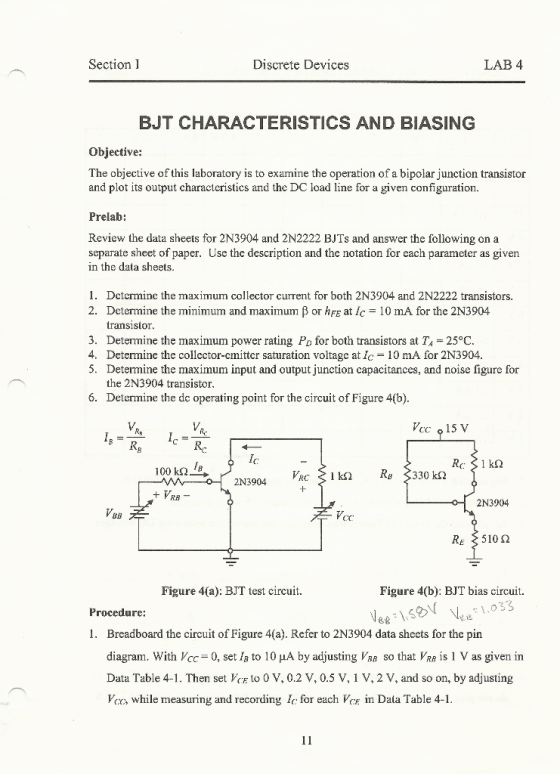
4. Lab VIII: Experiment VII The Bipolar Junction Transistor (BJT) Characteristics The bipolar junction transistor (BJT)...
 4. Lab VIII: Experiment VII The Bipolar Junction Transistor (BJT) Characteristics The bipolar junction transistor (BJT) is a three-terminal solid state device widely used as an amplifier (or switching) device. It consists of two n-type materials sandwiched by p-type material (npn) or two p-type and n-type. The terminals (sections) are known as emitter E, base B and collector C. Two currents and two voltages uniquely describe the behavior of the device. The third current/voltage can be determined through KCL/KVL. See...
EXERCISES 8.12 For the circuit in Fig. 8. 19, let 1-1 m1A, Vcc-15 VR-|0 kQ, with α 1, and let the...
 EXERCISES 8.12 For the circuit in Fig. 8. 19, let 1-1 m1A, Vcc-15 VR-|0 kQ, with α 1, and let the input voltages be: t'ai = 5 + 0.005 sin 2π × 1000t. volts, and = 5-0.005 sin 2π × 10001, volts. (a) If the BJTs are specified to have gr of 0.7 V at a collector current of 1 mA. find the voltage at the emitters. (b) Find g, for each of the two transistors. (c) Find ic for...
draw a base biased circuit and refered to question 5 and complete table. please draw the fixed bias diagram circuit and follow throught step on the next question. Figure 1. Bipolar junction tran...
 draw a base biased circuit and refered to question 5 and
complete table.
please draw the fixed bias diagram circuit and follow throught step
on the next question.
Figure 1. Bipolar junction transistor under base bias/fixed bias 5. In the circuit drawn in Figure 1, label the components with the following values: Base voltage, Collector voltage10V Base resistance Collector resistance Base - emitter voltage 2.7 k2 0.7 V 160 6. Connect the circuit drawn in Figure 1 on the breadboard....
draw a base biased circuit and refered to question 5 and
complete table.
please draw the fixed bias diagram circuit and follow throught step
on the next question.
Figure 1. Bipolar junction transistor under base bias/fixed bias 5. In the circuit drawn in Figure 1, label the components with the following values: Base voltage, Collector voltage10V Base resistance Collector resistance Base - emitter voltage 2.7 k2 0.7 V 160 6. Connect the circuit drawn in Figure 1 on the breadboard....
Problem: In the circuit shown in Figure 1, Vee = 1.2 V, Vcc = 20 V,...
 Problem: In the circuit shown in Figure 1, Vee = 1.2 V, Vcc = 20 V, Rp = 60 kN, Rc = 2 k. The input signal is a sinusoidal voltage given by Vin(t) = 0.2 sin(2000 ) V. The input and output characteristics of the transistor are provided on Page 2. (1) Find Ig, Ic and Vce. (30 points) Hint: Use the load line method. (Vor.) and (Vce: 1c) are the operating points of the transistor in the input...
I keep getting the wrong answer from everyone else pls help me get the right answer...
 I keep getting the wrong answer from everyone else pls help me
get the right answer
For the BJT bias circuit shown, what value of Rc in kilohms is needed to allow the maximum possible peak-to-peak signal swing on the collector without clipping? Use Vcc-9V, Vee--7V, Vb-1.2V, and Re -9.9k2. Assume that to keep the transistor in the forward-active region, the base-collector junction cannot be forward biased. Use B 20 and Vbe(on) 0.7V. Neglect the effects of base-width modulation. Vcc...
I keep getting the wrong answer from everyone else pls help me
get the right answer
For the BJT bias circuit shown, what value of Rc in kilohms is needed to allow the maximum possible peak-to-peak signal swing on the collector without clipping? Use Vcc-9V, Vee--7V, Vb-1.2V, and Re -9.9k2. Assume that to keep the transistor in the forward-active region, the base-collector junction cannot be forward biased. Use B 20 and Vbe(on) 0.7V. Neglect the effects of base-width modulation. Vcc...
Design the BJT current mirror shown in Figure 1 to replicate a 1 mA reference current at the coll...
 Ignore PSpice Simulation
Design the BJT current mirror shown in Figure 1 to replicate a 1 mA reference current at the collector of 02. Assume a scale current of 6.7 fA, V 74 V, and B-200. 1. Determine Ri such that IREF- 1 mA is the current, Ic, flowing into the collector of Qi 2. Calculate Io/IREF, where Io- Ic2. 3. Simulate the circuit in Figure 1 in PSpice. Use the SEDRA_LIB library for the Q2N3904 and enter the appropriate...
Ignore PSpice Simulation
Design the BJT current mirror shown in Figure 1 to replicate a 1 mA reference current at the collector of 02. Assume a scale current of 6.7 fA, V 74 V, and B-200. 1. Determine Ri such that IREF- 1 mA is the current, Ic, flowing into the collector of Qi 2. Calculate Io/IREF, where Io- Ic2. 3. Simulate the circuit in Figure 1 in PSpice. Use the SEDRA_LIB library for the Q2N3904 and enter the appropriate...
 Download the datasheet for 2N3904 and find the value of Bp. (Hint: Use average value) Be= Voc +10 V RB We are going to consider the common emitter configuration circuit shown in the figure to test a 2N3904 npn Bipolar Junction Transistor (BJT) under DC bias conditions. Your circuit should place a fixed collector resistor, Rc, in the circuit to prevent the collector current, Ic, from exceeding 40 mA (for this, you know that the minimum value of is zero)....
 I need help filling out the table, please let me know if any
of the values are wrong - the link to the data sheet is at the
bottom in red. There are 2 corresponding questions too, thank
you!
Download the manufacturer datasheet for the 2N3904 and fill in the values in the table below: Table 1: 2N3904 BJT manufacture's parameters Max. collector current 200 mA DC Max.power dissipation Max. junction voltages: C-E, C-B, E-B Typical value of Vce in...
I need help filling out the table, please let me know if any
of the values are wrong - the link to the data sheet is at the
bottom in red. There are 2 corresponding questions too, thank
you!
Download the manufacturer datasheet for the 2N3904 and fill in the values in the table below: Table 1: 2N3904 BJT manufacture's parameters Max. collector current 200 mA DC Max.power dissipation Max. junction voltages: C-E, C-B, E-B Typical value of Vce in...
 I keep getting the wrong answer from everyone else pls help me
get the right answer
For the BJT bias circuit shown, what value of Rc in kilohms is needed to allow the maximum possible peak-to-peak signal swing on the collector without clipping? Use Vcc-9V, Vee--7V, Vb-1.2V, and Re -9.9k2. Assume that to keep the transistor in the forward-active region, the base-collector junction cannot be forward biased. Use B 20 and Vbe(on) 0.7V. Neglect the effects of base-width modulation. Vcc...
I keep getting the wrong answer from everyone else pls help me
get the right answer
For the BJT bias circuit shown, what value of Rc in kilohms is needed to allow the maximum possible peak-to-peak signal swing on the collector without clipping? Use Vcc-9V, Vee--7V, Vb-1.2V, and Re -9.9k2. Assume that to keep the transistor in the forward-active region, the base-collector junction cannot be forward biased. Use B 20 and Vbe(on) 0.7V. Neglect the effects of base-width modulation. Vcc...
 QUESTION4 Total 24 Marks] For the amplifier circuit shown in Figure 4, assume the input signal V has zero DC component. Assume both transistors have p-100. (a) State the type of feedback topology used in the amplifier circuit and which type of 12 marks] amplifier is shown in the figure. (b Determine the DC voltages at all nodes of transistors Q1 and Q2. and the DC currents 18 marks] at the emitters of transistors Q1 and Q2 (c) Use the...
 4. Lab VIII: Experiment VII The Bipolar Junction Transistor (BJT) Characteristics The bipolar junction transistor (BJT) is a three-terminal solid state device widely used as an amplifier (or switching) device. It consists of two n-type materials sandwiched by p-type material (npn) or two p-type and n-type. The terminals (sections) are known as emitter E, base B and collector C. Two currents and two voltages uniquely describe the behavior of the device. The third current/voltage can be determined through KCL/KVL. See...
 EXERCISES 8.12 For the circuit in Fig. 8. 19, let 1-1 m1A, Vcc-15 VR-|0 kQ, with α 1, and let the input voltages be: t'ai = 5 + 0.005 sin 2π × 1000t. volts, and = 5-0.005 sin 2π × 10001, volts. (a) If the BJTs are specified to have gr of 0.7 V at a collector current of 1 mA. find the voltage at the emitters. (b) Find g, for each of the two transistors. (c) Find ic for...
 draw a base biased circuit and refered to question 5 and
complete table.
please draw the fixed bias diagram circuit and follow throught step
on the next question.
Figure 1. Bipolar junction transistor under base bias/fixed bias 5. In the circuit drawn in Figure 1, label the components with the following values: Base voltage, Collector voltage10V Base resistance Collector resistance Base - emitter voltage 2.7 k2 0.7 V 160 6. Connect the circuit drawn in Figure 1 on the breadboard....
draw a base biased circuit and refered to question 5 and
complete table.
please draw the fixed bias diagram circuit and follow throught step
on the next question.
Figure 1. Bipolar junction transistor under base bias/fixed bias 5. In the circuit drawn in Figure 1, label the components with the following values: Base voltage, Collector voltage10V Base resistance Collector resistance Base - emitter voltage 2.7 k2 0.7 V 160 6. Connect the circuit drawn in Figure 1 on the breadboard....
 Problem: In the circuit shown in Figure 1, Vee = 1.2 V, Vcc = 20 V, Rp = 60 kN, Rc = 2 k. The input signal is a sinusoidal voltage given by Vin(t) = 0.2 sin(2000 ) V. The input and output characteristics of the transistor are provided on Page 2. (1) Find Ig, Ic and Vce. (30 points) Hint: Use the load line method. (Vor.) and (Vce: 1c) are the operating points of the transistor in the input...
 I keep getting the wrong answer from everyone else pls help me
get the right answer
For the BJT bias circuit shown, what value of Rc in kilohms is needed to allow the maximum possible peak-to-peak signal swing on the collector without clipping? Use Vcc-9V, Vee--7V, Vb-1.2V, and Re -9.9k2. Assume that to keep the transistor in the forward-active region, the base-collector junction cannot be forward biased. Use B 20 and Vbe(on) 0.7V. Neglect the effects of base-width modulation. Vcc...
I keep getting the wrong answer from everyone else pls help me
get the right answer
For the BJT bias circuit shown, what value of Rc in kilohms is needed to allow the maximum possible peak-to-peak signal swing on the collector without clipping? Use Vcc-9V, Vee--7V, Vb-1.2V, and Re -9.9k2. Assume that to keep the transistor in the forward-active region, the base-collector junction cannot be forward biased. Use B 20 and Vbe(on) 0.7V. Neglect the effects of base-width modulation. Vcc...
 Ignore PSpice Simulation
Design the BJT current mirror shown in Figure 1 to replicate a 1 mA reference current at the collector of 02. Assume a scale current of 6.7 fA, V 74 V, and B-200. 1. Determine Ri such that IREF- 1 mA is the current, Ic, flowing into the collector of Qi 2. Calculate Io/IREF, where Io- Ic2. 3. Simulate the circuit in Figure 1 in PSpice. Use the SEDRA_LIB library for the Q2N3904 and enter the appropriate...
Ignore PSpice Simulation
Design the BJT current mirror shown in Figure 1 to replicate a 1 mA reference current at the collector of 02. Assume a scale current of 6.7 fA, V 74 V, and B-200. 1. Determine Ri such that IREF- 1 mA is the current, Ic, flowing into the collector of Qi 2. Calculate Io/IREF, where Io- Ic2. 3. Simulate the circuit in Figure 1 in PSpice. Use the SEDRA_LIB library for the Q2N3904 and enter the appropriate...
Most questions answered within 3 hours.
-
A cell biologist interested in the transport of calcium ions
(Ca2+) across the plasma membrane of...
asked 1 minute ago -
Suppose the average time it takes to drive from SFSU to Redwood
City is 41 minutes,...
asked 7 minutes ago -
The more formal name for a balance sheet is:
A) statement of net worth
B) statement...
asked 4 minutes ago -
In
stable industries, such as retailers, the gross profit is generally
volatile from year to year?
asked 7 minutes ago -
Two identical positive point charges (q1 = q2 = +2.00 nC) are
placed at the bottom...
asked 8 minutes ago -
1. When you a place a rubber loose rubber band in contact with
your lip, you...
asked 9 minutes ago -
In 500 words or more, explain PCI compliance to the
database administrator at a large retailer....
asked 21 minutes ago -
Find
z0
such that
P(−z0 < z < z0) = 0.6.
(Round your answer to two...
asked 26 minutes ago -
a) The Sarbanes-Oxley Act of 2002 has been most pertinent and
transformative to management decision making...
asked 35 minutes ago -
A driver travels northbound on a highway at a speed of 24.0 m/s.
A police car,...
asked 41 minutes ago -
There are three things that contribute to the significance of
differences. The following is NOT one...
asked 47 minutes ago -
A glowing blackbody is at a temperature of 4.325×10³ K. For this
temperature the peak in...
asked 54 minutes ago