


Homework Answers
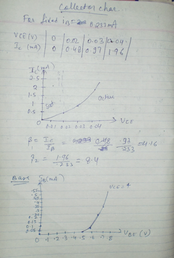
Collector Characteristics
Test 1: VBB=3.0 volt
Vcc(v) 0 0.5 1 2 3 4 6 8 10 12 VCE(v) 0 0.02 0.03 0.04 0.04 0.05 0.05 0.06 0.06 0.07 VRB(v) 2.33 2.33 2.33 2.33 2.33 2.29 2.28 2.27 2.27 2.26 IC(mA) 0 0.48 0.97 1.96 2.96 3.95 5.95 7.94 9.94 11.93 IB(mA) 0.233 0.233 0.233 0.233 0.233 0.229 0.228 0.227 0.227 0.226Test 2: VBB=2.0 volt
Vcc(v) 0 0.5 1 2 3 4 6 8 10 12 VCE(v) 0 0.03 0.04 0.05 0.06 0.06 0.07 0.07 0.09 0.09 VRB(v) 1.35 1.34 1.33 1.32 1.31 1.3 1.29 1.28 1.27 1.27 IC(mA) 0 0.47 0.96 1.95 2.94 3.94 5.93 7.93 9.91 11.91 IB(mA) 0.135 0.134 0.133 0.132 0.131 0.13 0.129 0.128 0.127 0.127Test 3: VBB=1.0 volt
Vcc(v) 0 0.5 1 2 3 4 6 8 10 12 VCE(v) 0 0.05 0.06 0.08 0.09 0.11 0.12 0.15 0.24 1.24 VRB(v) 0.39 0.36 0.35 0.33 0.32 0.31 0.3 0.29 0.29 0.29 IC(mA) 0 0.45 0.94 1.92 2.91 3.89 5.88 7.85 9.76 10.76 IB(mA) 0.039 0.036 0.035 0.033 0.032 0.031 0.03 0.029 0.029 0.029Test 4: VBB=0 volt
Vcc(v) 0 0.5 1 2 3 4 6 8 10 12 VCE(v) 0 0.5 1 2 3 4 6 8 10 12 VRB(v) 0 0 0 0 0 0 0 0 0 0 IC(mA) 0 0 0 0 0 0 0 0 0 0 IB(mA) 0 0 0 0 0 0 0 0 0 0Base Characteristics
VCC=8 volt
| VBB(v) | 0 | 0.5 | 1 | 2 | 3 | 4 | 6 | 8 | 10 | 12 |
| VCE(v) | 8 | 8 | 0.15 | 0.07 | 0.06 | 0.05 | 0.04 | 0.03 | 0.03 | 0.02 |
| VBE(v) | 0 | 0.5 | 0.71 | 0.72 | 0.73 | 0.73 | 0.73 | 0.73 | 0.73 | 0.73 |
| IC(mA) | 0 | 0 | 7.85 | 7.93 | 7.94 | 7.95 | 7.96 | 7.97 | 7.97 | 7.98 |
| IB(mA) | 0 | 0 | 0.029 | 0.128 | 0.227 | 0.327 | 0.527 | 0.727 | 0.927 | 1.127 |
VCC=4volt
| VBB(v) | 0 | 0.5 | 1 | 2 | 3 | 4 | 6 | 8 | 10 | 12 |
| VCE(v) | 0.4 | 0.4 | 0.11 | 0.06 | 0.05 | 0.04 | 0.04 | 0.03 | 0.03 | 0.03 |
| VBE(v) | 0 | 0 | 0.68 | 0.7 | 0.71 | 0.71 | 0.71 | 0.71 | 0.71 | 0.71 |
| IC(mA) | 3.6 | 3.6 | 3.89 | 3.94 | 3.95 | 3.96 | 3.96 | 3.97 | 3.97 | 3.97 |
| IB(mA) | 0 | 0.05 | 0.032 | 0.13 | 0.229 | 0.329 | 0.529 | 0.729 | 0.929 | 1.129 |
VCC=0 volt
| VBB(v) | 0 | 0.5 | 1 | 2 | 3 | 4 | 6 | 8 | 10 | 12 |
| VCE(v) | 4 | 4 | 4 | 4 | 4 | 4 | 4 | 4 | 4 | 4 |
| VBE(v) | 0 | 0.5 | 0.61 | 0.65 | 0.67 | 0.68 | 0.69 | 0.7 | 0.7 | 0.7 |
| IC(mA) | -4 | -4 | -4 | -4 | -4 | -4 | -4 | -4 | -4 | -4 |
| IB(mA) | 0 | 0 | 0.039 | 0.135 | 0.233 | 0.332 | 0.531 | 0.73 | 0.93 | 1.13 |
Add Answer to:
4. Lab VIII: Experiment VII The Bipolar Junction Transistor (BJT) Characteristics The bipolar junction transistor (BJT)...
Please only use PSpice as stated in the directions. Any other software will not be accepted....
 Please only use PSpice as stated in the directions. Any other
software will not be accepted. Thanks
No multisim or LTSpice.
Part I: Transistor Output Characteristic Procedure: 1. Build the circuit model in PSpice as shown in Fig. 1 with Vbb = 10V, R2 = 330 k92 and R3 = 0.22 k22. R3 0.22 Vec vbь R2 Q1 10V 330k or 147k Figure 1. Circuit configuration for Transistor output characteristic testing 2. Use Ohm's Law to calculate Ib. You may...
Please only use PSpice as stated in the directions. Any other
software will not be accepted. Thanks
No multisim or LTSpice.
Part I: Transistor Output Characteristic Procedure: 1. Build the circuit model in PSpice as shown in Fig. 1 with Vbb = 10V, R2 = 330 k92 and R3 = 0.22 k22. R3 0.22 Vec vbь R2 Q1 10V 330k or 147k Figure 1. Circuit configuration for Transistor output characteristic testing 2. Use Ohm's Law to calculate Ib. You may...
Consider the BJT common-emitter amplifier in Figure 1. Assume that the 2N3904G transistor has the following parameters: β-206, VBE-0.TV and the Early voltage VAT 1000V. vCC RB1a I multiple resistors...
 Consider the BJT common-emitter amplifier in Figure 1. Assume that the 2N3904G transistor has the following parameters: β-206, VBE-0.TV and the Early voltage VAT 1000V. vCC RB1a I multiple resistors RC want n Vload 22HF Rload 01 2N3904G V1 6302 4.7HF RE2CE 0.01Vpk 1kHz maliple esistons lue you available in the ki Figure 1 BJT CE amplifier 0.5 V and VC-3 V (a) Design the DC biasing circuit so that lc-2 mA, VCE = 2.5 V, VE
Consider the BJT...
Consider the BJT common-emitter amplifier in Figure 1. Assume that the 2N3904G transistor has the following parameters: β-206, VBE-0.TV and the Early voltage VAT 1000V. vCC RB1a I multiple resistors RC want n Vload 22HF Rload 01 2N3904G V1 6302 4.7HF RE2CE 0.01Vpk 1kHz maliple esistons lue you available in the ki Figure 1 BJT CE amplifier 0.5 V and VC-3 V (a) Design the DC biasing circuit so that lc-2 mA, VCE = 2.5 V, VE
Consider the BJT...
ASAP! Question 1 [Soalan 1] (a) Describe the condition when a npn BJT transistor operates in...
 ASAP!
Question 1 [Soalan 1] (a) Describe the condition when a npn BJT transistor operates in saturation condition and what are the terminal currents and voltages conditions during saturation. [Terangkan keadaan bila satu transistor BJT npn beroperasi dalam keadaan tepu dan apakah keadaan arus dan voltan terminal semasa tepu. ] (20 Marks/Markah) (b) Consider the BJT transistor circuit in Figure 1. If Bpc = 100 and VBE = 0.65V, calculate: [Pertimbangkan litar transistor BJT dalam Rajah 1. Jika Bpc =...
ASAP!
Question 1 [Soalan 1] (a) Describe the condition when a npn BJT transistor operates in saturation condition and what are the terminal currents and voltages conditions during saturation. [Terangkan keadaan bila satu transistor BJT npn beroperasi dalam keadaan tepu dan apakah keadaan arus dan voltan terminal semasa tepu. ] (20 Marks/Markah) (b) Consider the BJT transistor circuit in Figure 1. If Bpc = 100 and VBE = 0.65V, calculate: [Pertimbangkan litar transistor BJT dalam Rajah 1. Jika Bpc =...
please choose one of the answer choices above. Must show all work, thank you Question 7...
 please choose one of the answer choices above.
Must show all work, thank you
Question 7 CIRCUIT D1 (2.5 Marks) Statement: Sketching relevant output (Vc-Ic) characteristics decide on Q-point coordinates and DC load-line details: That is, determine DC operating conditions of the NPN-BJT/Si circuit of Fig. 7 (denoting the type Circuit C2). Assume the following: Vcc= 18 volt; VBE = 0.7; Rc = 1.5 k; RB2 = 33 k; Vc = 9.5 volt; Irc = 9.5 and, B = 100...
please choose one of the answer choices above.
Must show all work, thank you
Question 7 CIRCUIT D1 (2.5 Marks) Statement: Sketching relevant output (Vc-Ic) characteristics decide on Q-point coordinates and DC load-line details: That is, determine DC operating conditions of the NPN-BJT/Si circuit of Fig. 7 (denoting the type Circuit C2). Assume the following: Vcc= 18 volt; VBE = 0.7; Rc = 1.5 k; RB2 = 33 k; Vc = 9.5 volt; Irc = 9.5 and, B = 100...
Could someone please help me on how I should be configuring the circuit in Figure 4(a)...
 Could someone please help me on how I should be configuring the
circuit in Figure 4(a) in Multisim? Basically not understanding
question #1 in the Procedure. Cannot keep Vrb the same value while
adjusting Vcc. Then when trying to adjust Vbb to hold Vrb, Ib
changes.
Any help is appreciated!
Discrete Devices Section LAB 4 BJT CHARACTERISTICS AND BIASING Objective: The objective of this laboratory is to examine the operation of a bipolar junction transistor and plot its output characteristics...
Could someone please help me on how I should be configuring the
circuit in Figure 4(a) in Multisim? Basically not understanding
question #1 in the Procedure. Cannot keep Vrb the same value while
adjusting Vcc. Then when trying to adjust Vbb to hold Vrb, Ib
changes.
Any help is appreciated!
Discrete Devices Section LAB 4 BJT CHARACTERISTICS AND BIASING Objective: The objective of this laboratory is to examine the operation of a bipolar junction transistor and plot its output characteristics...
Post lab 1. From the experimental data in tables 1 and 2, obtain the following; a....
 Post lab 1. From the experimental data in tables 1 and 2, obtain the following; a. Input characteristics - plots of VBE (x-axis) vs Ib (y-axis) with constant values VCE b. Output characteristics - plots of VCE (x-axis) vs Ic (y- axis) with constant values of Ib. c. Dynamic input resistance and output resistance 2. DC current gain () of the transistor and compare this value with that of the value given in the datasheet. 3. What are the uses...
Download the datasheet for 2N3904 and find the value of Bp. (Hint: Use average value) Be=...
 Download the datasheet for 2N3904 and find the value of Bp. (Hint: Use average value) Be= Voc +10 V RB We are going to consider the common emitter configuration circuit shown in the figure to test a 2N3904 npn Bipolar Junction Transistor (BJT) under DC bias conditions. Your circuit should place a fixed collector resistor, Rc, in the circuit to prevent the collector current, Ic, from exceeding 40 mA (for this, you know that the minimum value of is zero)....
Please show clear work and separate each question. other answers on here are a joke to...
 Please show clear work and separate each question. other answers
on here are a joke to try and follow.
1) For the circuit and I-V characteristic shown, draw the loadline. Find is and VCE for VBB = 1 V, 1.5 V, and 2 V. (RB = 30 KS2, and assume VBE=0.7 V). Solve this graphically. ic (mA) qVcc = +10 V -ig = 140 MA &R c = 1.25k2 120 MA ce R on + 80 A VAT -40 MA...
Please show clear work and separate each question. other answers
on here are a joke to try and follow.
1) For the circuit and I-V characteristic shown, draw the loadline. Find is and VCE for VBB = 1 V, 1.5 V, and 2 V. (RB = 30 KS2, and assume VBE=0.7 V). Solve this graphically. ic (mA) qVcc = +10 V -ig = 140 MA &R c = 1.25k2 120 MA ce R on + 80 A VAT -40 MA...
question 3 and 4 Problem2 (30 points) Consider an npn bipolar transistor with the following characteristics...
 question 3 and 4
Problem2 (30 points) Consider an npn bipolar transistor with the following characteristics Base Collector Emitter Na-5x 1016 cm3 Ng- 1015 cm3 N1018 cm3 DC- 12 cm-/sec DE 8 cm-/sec (diff coef.) DB 15 cm-/sec sec TEO 108 sec (life time) tB0 5x 10 tCo 10 sec xp 0.7 um (Base width) xg 0.8 um (emitter width) D Remember D/u= KT /q, and L n.p n.p A forward bias of 0.5 V is applied to the emitter-base...
question 3 and 4
Problem2 (30 points) Consider an npn bipolar transistor with the following characteristics Base Collector Emitter Na-5x 1016 cm3 Ng- 1015 cm3 N1018 cm3 DC- 12 cm-/sec DE 8 cm-/sec (diff coef.) DB 15 cm-/sec sec TEO 108 sec (life time) tB0 5x 10 tCo 10 sec xp 0.7 um (Base width) xg 0.8 um (emitter width) D Remember D/u= KT /q, and L n.p n.p A forward bias of 0.5 V is applied to the emitter-base...
EXERCISES 8.12 For the circuit in Fig. 8. 19, let 1-1 m1A, Vcc-15 VR-|0 kQ, with α 1, and let the...
 EXERCISES 8.12 For the circuit in Fig. 8. 19, let 1-1 m1A, Vcc-15 VR-|0 kQ, with α 1, and let the input voltages be: t'ai = 5 + 0.005 sin 2π × 1000t. volts, and = 5-0.005 sin 2π × 10001, volts. (a) If the BJTs are specified to have gr of 0.7 V at a collector current of 1 mA. find the voltage at the emitters. (b) Find g, for each of the two transistors. (c) Find ic for...
 Please only use PSpice as stated in the directions. Any other
software will not be accepted. Thanks
No multisim or LTSpice.
Part I: Transistor Output Characteristic Procedure: 1. Build the circuit model in PSpice as shown in Fig. 1 with Vbb = 10V, R2 = 330 k92 and R3 = 0.22 k22. R3 0.22 Vec vbь R2 Q1 10V 330k or 147k Figure 1. Circuit configuration for Transistor output characteristic testing 2. Use Ohm's Law to calculate Ib. You may...
Please only use PSpice as stated in the directions. Any other
software will not be accepted. Thanks
No multisim or LTSpice.
Part I: Transistor Output Characteristic Procedure: 1. Build the circuit model in PSpice as shown in Fig. 1 with Vbb = 10V, R2 = 330 k92 and R3 = 0.22 k22. R3 0.22 Vec vbь R2 Q1 10V 330k or 147k Figure 1. Circuit configuration for Transistor output characteristic testing 2. Use Ohm's Law to calculate Ib. You may...
 Consider the BJT common-emitter amplifier in Figure 1. Assume that the 2N3904G transistor has the following parameters: β-206, VBE-0.TV and the Early voltage VAT 1000V. vCC RB1a I multiple resistors RC want n Vload 22HF Rload 01 2N3904G V1 6302 4.7HF RE2CE 0.01Vpk 1kHz maliple esistons lue you available in the ki Figure 1 BJT CE amplifier 0.5 V and VC-3 V (a) Design the DC biasing circuit so that lc-2 mA, VCE = 2.5 V, VE
Consider the BJT...
Consider the BJT common-emitter amplifier in Figure 1. Assume that the 2N3904G transistor has the following parameters: β-206, VBE-0.TV and the Early voltage VAT 1000V. vCC RB1a I multiple resistors RC want n Vload 22HF Rload 01 2N3904G V1 6302 4.7HF RE2CE 0.01Vpk 1kHz maliple esistons lue you available in the ki Figure 1 BJT CE amplifier 0.5 V and VC-3 V (a) Design the DC biasing circuit so that lc-2 mA, VCE = 2.5 V, VE
Consider the BJT...
 ASAP!
Question 1 [Soalan 1] (a) Describe the condition when a npn BJT transistor operates in saturation condition and what are the terminal currents and voltages conditions during saturation. [Terangkan keadaan bila satu transistor BJT npn beroperasi dalam keadaan tepu dan apakah keadaan arus dan voltan terminal semasa tepu. ] (20 Marks/Markah) (b) Consider the BJT transistor circuit in Figure 1. If Bpc = 100 and VBE = 0.65V, calculate: [Pertimbangkan litar transistor BJT dalam Rajah 1. Jika Bpc =...
ASAP!
Question 1 [Soalan 1] (a) Describe the condition when a npn BJT transistor operates in saturation condition and what are the terminal currents and voltages conditions during saturation. [Terangkan keadaan bila satu transistor BJT npn beroperasi dalam keadaan tepu dan apakah keadaan arus dan voltan terminal semasa tepu. ] (20 Marks/Markah) (b) Consider the BJT transistor circuit in Figure 1. If Bpc = 100 and VBE = 0.65V, calculate: [Pertimbangkan litar transistor BJT dalam Rajah 1. Jika Bpc =...
 please choose one of the answer choices above.
Must show all work, thank you
Question 7 CIRCUIT D1 (2.5 Marks) Statement: Sketching relevant output (Vc-Ic) characteristics decide on Q-point coordinates and DC load-line details: That is, determine DC operating conditions of the NPN-BJT/Si circuit of Fig. 7 (denoting the type Circuit C2). Assume the following: Vcc= 18 volt; VBE = 0.7; Rc = 1.5 k; RB2 = 33 k; Vc = 9.5 volt; Irc = 9.5 and, B = 100...
please choose one of the answer choices above.
Must show all work, thank you
Question 7 CIRCUIT D1 (2.5 Marks) Statement: Sketching relevant output (Vc-Ic) characteristics decide on Q-point coordinates and DC load-line details: That is, determine DC operating conditions of the NPN-BJT/Si circuit of Fig. 7 (denoting the type Circuit C2). Assume the following: Vcc= 18 volt; VBE = 0.7; Rc = 1.5 k; RB2 = 33 k; Vc = 9.5 volt; Irc = 9.5 and, B = 100...
 Could someone please help me on how I should be configuring the
circuit in Figure 4(a) in Multisim? Basically not understanding
question #1 in the Procedure. Cannot keep Vrb the same value while
adjusting Vcc. Then when trying to adjust Vbb to hold Vrb, Ib
changes.
Any help is appreciated!
Discrete Devices Section LAB 4 BJT CHARACTERISTICS AND BIASING Objective: The objective of this laboratory is to examine the operation of a bipolar junction transistor and plot its output characteristics...
Could someone please help me on how I should be configuring the
circuit in Figure 4(a) in Multisim? Basically not understanding
question #1 in the Procedure. Cannot keep Vrb the same value while
adjusting Vcc. Then when trying to adjust Vbb to hold Vrb, Ib
changes.
Any help is appreciated!
Discrete Devices Section LAB 4 BJT CHARACTERISTICS AND BIASING Objective: The objective of this laboratory is to examine the operation of a bipolar junction transistor and plot its output characteristics...
 Post lab 1. From the experimental data in tables 1 and 2, obtain the following; a. Input characteristics - plots of VBE (x-axis) vs Ib (y-axis) with constant values VCE b. Output characteristics - plots of VCE (x-axis) vs Ic (y- axis) with constant values of Ib. c. Dynamic input resistance and output resistance 2. DC current gain () of the transistor and compare this value with that of the value given in the datasheet. 3. What are the uses...
 Download the datasheet for 2N3904 and find the value of Bp. (Hint: Use average value) Be= Voc +10 V RB We are going to consider the common emitter configuration circuit shown in the figure to test a 2N3904 npn Bipolar Junction Transistor (BJT) under DC bias conditions. Your circuit should place a fixed collector resistor, Rc, in the circuit to prevent the collector current, Ic, from exceeding 40 mA (for this, you know that the minimum value of is zero)....
 Please show clear work and separate each question. other answers
on here are a joke to try and follow.
1) For the circuit and I-V characteristic shown, draw the loadline. Find is and VCE for VBB = 1 V, 1.5 V, and 2 V. (RB = 30 KS2, and assume VBE=0.7 V). Solve this graphically. ic (mA) qVcc = +10 V -ig = 140 MA &R c = 1.25k2 120 MA ce R on + 80 A VAT -40 MA...
Please show clear work and separate each question. other answers
on here are a joke to try and follow.
1) For the circuit and I-V characteristic shown, draw the loadline. Find is and VCE for VBB = 1 V, 1.5 V, and 2 V. (RB = 30 KS2, and assume VBE=0.7 V). Solve this graphically. ic (mA) qVcc = +10 V -ig = 140 MA &R c = 1.25k2 120 MA ce R on + 80 A VAT -40 MA...
 question 3 and 4
Problem2 (30 points) Consider an npn bipolar transistor with the following characteristics Base Collector Emitter Na-5x 1016 cm3 Ng- 1015 cm3 N1018 cm3 DC- 12 cm-/sec DE 8 cm-/sec (diff coef.) DB 15 cm-/sec sec TEO 108 sec (life time) tB0 5x 10 tCo 10 sec xp 0.7 um (Base width) xg 0.8 um (emitter width) D Remember D/u= KT /q, and L n.p n.p A forward bias of 0.5 V is applied to the emitter-base...
question 3 and 4
Problem2 (30 points) Consider an npn bipolar transistor with the following characteristics Base Collector Emitter Na-5x 1016 cm3 Ng- 1015 cm3 N1018 cm3 DC- 12 cm-/sec DE 8 cm-/sec (diff coef.) DB 15 cm-/sec sec TEO 108 sec (life time) tB0 5x 10 tCo 10 sec xp 0.7 um (Base width) xg 0.8 um (emitter width) D Remember D/u= KT /q, and L n.p n.p A forward bias of 0.5 V is applied to the emitter-base...
 EXERCISES 8.12 For the circuit in Fig. 8. 19, let 1-1 m1A, Vcc-15 VR-|0 kQ, with α 1, and let the input voltages be: t'ai = 5 + 0.005 sin 2π × 1000t. volts, and = 5-0.005 sin 2π × 10001, volts. (a) If the BJTs are specified to have gr of 0.7 V at a collector current of 1 mA. find the voltage at the emitters. (b) Find g, for each of the two transistors. (c) Find ic for...
Most questions answered within 3 hours.
-
Which of the following pairs of ions have the same electron
configuration?
I: Br− and Se2−...
asked 8 minutes ago -
The Foremost Composite Materials Company is planning a two-day
sales conference for October 19-20. The conference...
asked 31 minutes ago -
3) Illustrate the observed pattern of relatedness of organisms
versus adaptations to specific conditions. This means...
asked 48 minutes ago -
In winter a lake has a 0.35 m thick ice layer over 1.10 m of
water....
asked 1 hour ago -
Assuming the following has been encrypted with a Vigenere cipher
below, use the method(s) and assumptions...
asked 2 hours ago -
How would I use switch statements to write a program that will
take an input of...
asked 2 hours ago -
Imagine a reaction in which methane gas combusts at a constant
pressure of 1 atm and...
asked 2 hours ago -
Two parallel wires (each 12 m in length) are separated by a
distance of 0.065 m...
asked 2 hours ago -
Suppose there were three masses at the corner of uniform
equilateral triangle. The masses are m1...
asked 2 hours ago -
Situation: A building that is 618 m above the ground floor. How
many times would a...
asked 2 hours ago -
help me and discuss one successful and one
unsuccessful international company/busines in Indonesia.whyit
succeed and why...
asked 2 hours ago -
I- Choose the best answer
Which of the following statements about the structure and
packaging of...
asked 2 hours ago