
VDD 0.9 v 03 24 IREF 200 μΑ 26 25 Qs Q, ks =-0.9 V Figure P8.106
Homework Answers


Add Answer to:
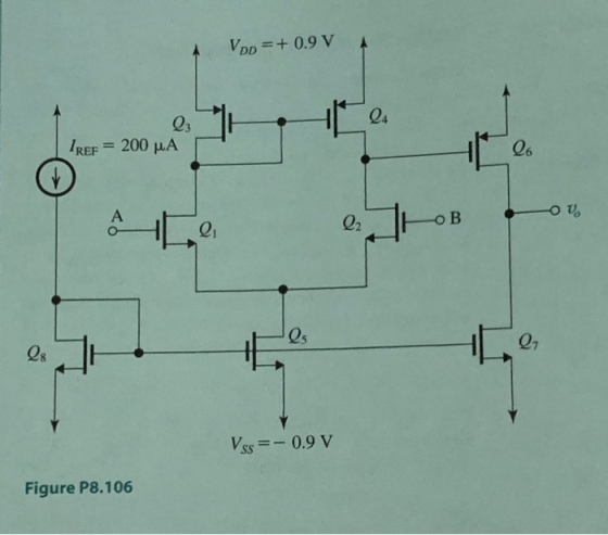
D 8.106 The two-stage CMOS op amp in Fig. P8.106 is fabricated in a 0.18-um technology having 4 k...
could you explain these equations cause i get confuse how do we get these? thanks in advance D 9.114 The two-stage CMO...
 could you explain these equations cause i get confuse
how do we get these?
thanks in advance
D 9.114 The two-stage CMOS op amp in Fig. P9.114 is D *9.115 In fabricated in a 0.18-μm technology having = 4 -Fig. 9.40 the increasing th of 4. Assumi (a) With A and B grounded, perform a dc design that will result in each of Q, Q2, Q3, and Q4 conducting a drain current of 100 1A and each of Q6 and...
could you explain these equations cause i get confuse
how do we get these?
thanks in advance
D 9.114 The two-stage CMOS op amp in Fig. P9.114 is D *9.115 In fabricated in a 0.18-μm technology having = 4 -Fig. 9.40 the increasing th of 4. Assumi (a) With A and B grounded, perform a dc design that will result in each of Q, Q2, Q3, and Q4 conducting a drain current of 100 1A and each of Q6 and...
Vo-stage CMOS op amp of the type of 3 has C, = 2 pF and is fabricated in a rocess characterized b...
 For good rating provide correct and full solution
vo-stage CMOS op amp of the type of 3 has C, = 2 pF and is fabricated in a rocess characterized by k- 65 0.02 V and f, , and λ,-0.05 v-1. If SR = 40 V/μs 25 MHz, find the bias current /ss of the SC input pair, the overdrive voltage Voy and the of the individual SC transistors, and the Ist-stage de gain a,o REF 4 FIGURE 5.13 Two-stage CMOS...
For good rating provide correct and full solution
vo-stage CMOS op amp of the type of 3 has C, = 2 pF and is fabricated in a rocess characterized by k- 65 0.02 V and f, , and λ,-0.05 v-1. If SR = 40 V/μs 25 MHz, find the bias current /ss of the SC input pair, the overdrive voltage Voy and the of the individual SC transistors, and the Ist-stage de gain a,o REF 4 FIGURE 5.13 Two-stage CMOS...
Q1: The cascode current source in Fig. 8.4.1 utilizes two identical PMOS transistors fabricated in a...
 Q1: The cascode current source in Fig. 8.4.1 utilizes two identical PMOS transistors fabricated in a V, 0.18-um CMOS process for which VDD 1.8 V pcor - 100 ???2 vG2 02 Design the circuit to obtain 1-50 ?? and Ro-I ?? and to allow for the maximum pos- sible voltage swing at the output terminal of the current source. Utilize Vov 0.2 V. Specify the 01 tor Gl ify the required values of the dc bias voltages VGI and VG2....
Hm emergency help, please IV. Two stage CMOS amplifier.(25 points) 0 are operated with overdrive voltages...
 Hm emergency help, please
IV. Two stage CMOS amplifier.(25 points) 0 are operated with overdrive voltages of 0,2-V magnitude; Qs and Q use overdrive voltages of o.5 V magnitude. The For s particular design of the two-stage CMOS op amp, 1.6- V supples are uwhied and all ransistors except for @ and econd stage is biased at 05 mA. The fabrication process employad provides - V. For all transistors the ength of the devices are 2.0 pm long and V-V-20...
Hm emergency help, please
IV. Two stage CMOS amplifier.(25 points) 0 are operated with overdrive voltages of 0,2-V magnitude; Qs and Q use overdrive voltages of o.5 V magnitude. The For s particular design of the two-stage CMOS op amp, 1.6- V supples are uwhied and all ransistors except for @ and econd stage is biased at 05 mA. The fabrication process employad provides - V. For all transistors the ength of the devices are 2.0 pm long and V-V-20...
voltage f an npn be? What and Ao becolle ned device in (c) is operated at 10 μΑ, find produce the st and highest values of A,? What are these values? (d) If the redesigned lor, g,1%, and Ao. Which de...
 voltage f an npn be? What and Ao becolle ned device in (c) is operated at 10 μΑ, find produce the st and highest values of A,? What are these values? (d) If the redesigned lor, g,1%, and Ao. Which designs and operating conditions Figure P7 39 cases, if WIL is held at the same value 7.40 The NMOS trans ricated in pendix K erated at l is made 10 times larger, what gains result? 36 Using a CMOS technology...
sedra smith book 7th edition chapter name is operational amplifier. question 12.1 to 12.10 I need...
 sedra smith book 7th edition chapter name is operational
amplifier. question 12.1 to 12.10 I need all solution with good
hand writing.
Problems 1075 Transistor Q3 WIL (um/um) 36/0.3 36/0.3 6/0.3 6/0.3 30/0.3 W/0.3 45/0.3 6/0.3 and A, if all devices are 0.3 m long, Q and Q2 are operated at overdrive voltages of 0.15-V magnitude, and Q is operated at Voy 0.2 V. Also, determine the op-amp output resistance 100 k2, C0.1 pF, G = 2 mA/V, R, =...
sedra smith book 7th edition chapter name is operational
amplifier. question 12.1 to 12.10 I need all solution with good
hand writing.
Problems 1075 Transistor Q3 WIL (um/um) 36/0.3 36/0.3 6/0.3 6/0.3 30/0.3 W/0.3 45/0.3 6/0.3 and A, if all devices are 0.3 m long, Q and Q2 are operated at overdrive voltages of 0.15-V magnitude, and Q is operated at Voy 0.2 V. Also, determine the op-amp output resistance 100 k2, C0.1 pF, G = 2 mA/V, R, =...
 could you explain these equations cause i get confuse
how do we get these?
thanks in advance
D 9.114 The two-stage CMOS op amp in Fig. P9.114 is D *9.115 In fabricated in a 0.18-μm technology having = 4 -Fig. 9.40 the increasing th of 4. Assumi (a) With A and B grounded, perform a dc design that will result in each of Q, Q2, Q3, and Q4 conducting a drain current of 100 1A and each of Q6 and...
could you explain these equations cause i get confuse
how do we get these?
thanks in advance
D 9.114 The two-stage CMOS op amp in Fig. P9.114 is D *9.115 In fabricated in a 0.18-μm technology having = 4 -Fig. 9.40 the increasing th of 4. Assumi (a) With A and B grounded, perform a dc design that will result in each of Q, Q2, Q3, and Q4 conducting a drain current of 100 1A and each of Q6 and...
 For good rating provide correct and full solution
vo-stage CMOS op amp of the type of 3 has C, = 2 pF and is fabricated in a rocess characterized by k- 65 0.02 V and f, , and λ,-0.05 v-1. If SR = 40 V/μs 25 MHz, find the bias current /ss of the SC input pair, the overdrive voltage Voy and the of the individual SC transistors, and the Ist-stage de gain a,o REF 4 FIGURE 5.13 Two-stage CMOS...
For good rating provide correct and full solution
vo-stage CMOS op amp of the type of 3 has C, = 2 pF and is fabricated in a rocess characterized by k- 65 0.02 V and f, , and λ,-0.05 v-1. If SR = 40 V/μs 25 MHz, find the bias current /ss of the SC input pair, the overdrive voltage Voy and the of the individual SC transistors, and the Ist-stage de gain a,o REF 4 FIGURE 5.13 Two-stage CMOS...
 Q1: The cascode current source in Fig. 8.4.1 utilizes two identical PMOS transistors fabricated in a V, 0.18-um CMOS process for which VDD 1.8 V pcor - 100 ???2 vG2 02 Design the circuit to obtain 1-50 ?? and Ro-I ?? and to allow for the maximum pos- sible voltage swing at the output terminal of the current source. Utilize Vov 0.2 V. Specify the 01 tor Gl ify the required values of the dc bias voltages VGI and VG2....
 Hm emergency help, please
IV. Two stage CMOS amplifier.(25 points) 0 are operated with overdrive voltages of 0,2-V magnitude; Qs and Q use overdrive voltages of o.5 V magnitude. The For s particular design of the two-stage CMOS op amp, 1.6- V supples are uwhied and all ransistors except for @ and econd stage is biased at 05 mA. The fabrication process employad provides - V. For all transistors the ength of the devices are 2.0 pm long and V-V-20...
Hm emergency help, please
IV. Two stage CMOS amplifier.(25 points) 0 are operated with overdrive voltages of 0,2-V magnitude; Qs and Q use overdrive voltages of o.5 V magnitude. The For s particular design of the two-stage CMOS op amp, 1.6- V supples are uwhied and all ransistors except for @ and econd stage is biased at 05 mA. The fabrication process employad provides - V. For all transistors the ength of the devices are 2.0 pm long and V-V-20...
 voltage f an npn be? What and Ao becolle ned device in (c) is operated at 10 μΑ, find produce the st and highest values of A,? What are these values? (d) If the redesigned lor, g,1%, and Ao. Which designs and operating conditions Figure P7 39 cases, if WIL is held at the same value 7.40 The NMOS trans ricated in pendix K erated at l is made 10 times larger, what gains result? 36 Using a CMOS technology...
 sedra smith book 7th edition chapter name is operational
amplifier. question 12.1 to 12.10 I need all solution with good
hand writing.
Problems 1075 Transistor Q3 WIL (um/um) 36/0.3 36/0.3 6/0.3 6/0.3 30/0.3 W/0.3 45/0.3 6/0.3 and A, if all devices are 0.3 m long, Q and Q2 are operated at overdrive voltages of 0.15-V magnitude, and Q is operated at Voy 0.2 V. Also, determine the op-amp output resistance 100 k2, C0.1 pF, G = 2 mA/V, R, =...
sedra smith book 7th edition chapter name is operational
amplifier. question 12.1 to 12.10 I need all solution with good
hand writing.
Problems 1075 Transistor Q3 WIL (um/um) 36/0.3 36/0.3 6/0.3 6/0.3 30/0.3 W/0.3 45/0.3 6/0.3 and A, if all devices are 0.3 m long, Q and Q2 are operated at overdrive voltages of 0.15-V magnitude, and Q is operated at Voy 0.2 V. Also, determine the op-amp output resistance 100 k2, C0.1 pF, G = 2 mA/V, R, =...
Most questions answered within 3 hours.
-
*****DO NOT ANSWER THIS QUESTION IF YOU DON'T
KNOW*******Rights and Duties of Auditors; Minimum 4000
words...
asked 27 minutes ago -
The probability that Janie is wearing sunglasses is 1/4. The
probability that she is wearing sunglasses...
asked 57 minutes ago -
Do you believe social media is more of a help or a hindrance in
controlling crises...
asked 1 hour ago -
Two long, parallel wires separated by 2.85 cm carry currents in
opposite directions. The current in...
asked 54 minutes ago -
Question # 1. Develop a list of rehabilitation journals
that publish articles concerning career counseling for...
asked 1 hour ago -
Bryant Company has a factory machine with a book value of
$85,100 and a remaining useful...
asked 1 hour ago -
What is the default classification for federal tax purposes of a
U.S. eligible entity with one...
asked 1 hour ago -
1. How many grams would 4.0x10²¹ atoms of calcium
weigh?
2.. Calculate the percent oxygen in...
asked 1 hour ago -
Balance Equation
K2Cr2O7 + H2C2O4 2H2O 6 K[Cr(C2O4 )2 (H2O)2 ]2H2O + CO2 +
H2O
asked 1 hour ago -
Select a position in the clinical laboratory and write an
appropriate job description and corresponding work...
asked 1 hour ago -
Targeting the Bottom of the Pyramid
What are some of the broader societal pricing concerns faced...
asked 1 hour ago -
Which of the following statements is correct? (3 marks)
a) Upon the public announcement of finding...
asked 1 hour ago