
Homework Answers
For the given State table, Draw the State Diagram:
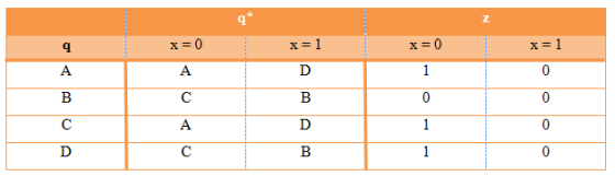
Given State Table:
State Diagram:

Timing trace for given input value:
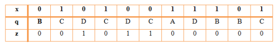
Timing Trace for given input is as shown above. Here, on input value of x and given current state, next state and output z is determined.
Trying to continue the Timing trace:

Add Answer to:
1) For the following state table, show a state diagram and complete the timing trace as far as po...
Show state diagram & Complete the timing trace q* z q x =0 x =1 x=0...
Show state diagram & Complete the timing trace q* z q x =0 x =1 x=0 x=1 A B C 0 1 B C A 0 0 C A B 1 0 x 0 0 1 1 1 0 0 0 0 0 1 0 q A z
Show the state transition diagram for a Moore system that produces a 1 output if and only if the ...
 Show the state transition
diagram for a Moore system that produces a 1 output if and only if
the input has been 0 1 1 for the last three clock times. A total of
4 states exist, and a sample timing trace is provided.
Extra Credit Problem 9 (5 pts): Show the state transition diagram for a Moore system that produces a 1 output if and only if the input has been 0 1 1 for the last three clock...
Show the state transition
diagram for a Moore system that produces a 1 output if and only if
the input has been 0 1 1 for the last three clock times. A total of
4 states exist, and a sample timing trace is provided.
Extra Credit Problem 9 (5 pts): Show the state transition diagram for a Moore system that produces a 1 output if and only if the input has been 0 1 1 for the last three clock...
Draw a state diagram and state table and show what if anything is wrong with the following synchronous state machine
 1. (a) Draw a state diagram and state table and show what if anything is wrong with the following synchronous state machine that has asynchronous input \(\mathrm{X}\) and state variables \(\mathrm{A} \& \mathrm{~B}\) ?(b) If possible, draw a new circuit (without adding or removing any flip-flops) that has the same functionality but fixes any problem with the circuit. Also, show the new state diagram and state table.
2. For the following digital design, (15%) Construct a state table, including output z Minty ritea Booleanexpress ons needed first. (10%) Complete the timing diagram for z. Assume flip-flop outpu...
 2. For the following digital design, (15%) Construct a state table, including output z Minty ritea Booleanexpress ons needed first. (10%) Complete the timing diagram for z. Assume flip-flop output is 0 initially. a. b. MUX 4i Clock Clock
2. For the following digital design, (15%) Construct a state table, including output z Minty ritea Booleanexpress ons needed first. (10%) Complete the timing diagram for z. Assume flip-flop output is 0 initially. a. b. MUX 4i Clock Clock
2. For the following digital design, (15%) Construct a state table, including output z Minty ritea Booleanexpress ons needed first. (10%) Complete the timing diagram for z. Assume flip-flop output is 0 initially. a. b. MUX 4i Clock Clock
please show your work. Fill in the state table for the following state diagram. Clearly label...
 please show your work.
Fill in the state table for the following state diagram. Clearly label each column with its usage (Present. Input, Output, Next). Use only as many rows as needed. 1 00 0 0 ( 11 QB 10 QA QB
please show your work.
Fill in the state table for the following state diagram. Clearly label each column with its usage (Present. Input, Output, Next). Use only as many rows as needed. 1 00 0 0 ( 11 QB 10 QA QB
Problem 3. (25 pts) The timing diagram for three state cases represents the high impedance state with a line between the low (0) and high (0) states, as ill figure: ustrated in the following 0 L...
 Problem 3. (25 pts) The timing diagram for three state cases represents the high impedance state with a line between the low (0) and high (0) states, as ill figure: ustrated in the following 0 Low (0) High Impedance (Z)1 High (1) a. (15 pts) Draw the timing diagrams for the outputs A,B,C,D of the following circuit given the input diagrams in the next page. (NOTE: to help you, dashed lines are shown for the different levels) b. (10 pts)...
Computer Organization and Design, Risc-V Mips Question 9 8 pts Complete the following trace of accesses to virtual addre...
 Computer Organization and Design, Risc-V Mips
Question 9 8 pts Complete the following trace of accesses to virtual addresses. In the case of page faults, continue allocating physical pages in the order Ox10000, 0x10001, Ox10002, etc. Page Physical Virtual Virtual TLB TLB PT Physical address page num hit/miss entry index fault page num address Ох00002040| Ох00002 Ox00011040 hit 2 Ox00011 OX000067CC Ox00006 Ox00080 0X000807CC miss 6 O no Ox00003008 Ox00003 Ох10000 miss 3 Ох10000008 1 yes Ox00005958 OX0000300C Ox00001080 OX00007F68...
Computer Organization and Design, Risc-V Mips
Question 9 8 pts Complete the following trace of accesses to virtual addresses. In the case of page faults, continue allocating physical pages in the order Ox10000, 0x10001, Ox10002, etc. Page Physical Virtual Virtual TLB TLB PT Physical address page num hit/miss entry index fault page num address Ох00002040| Ох00002 Ox00011040 hit 2 Ox00011 OX000067CC Ox00006 Ox00080 0X000807CC miss 6 O no Ox00003008 Ox00003 Ох10000 miss 3 Ох10000008 1 yes Ox00005958 OX0000300C Ox00001080 OX00007F68...
(20 points) Using any state encodings you want, generate a state table for the following state diagram. Note that there...
 (20 points) Using any state encodings you want, generate a state table for the following state diagram. Note that there is one input, X, and there are two outputs, Y and Z. You can come up with whatever names you want for your state variables. And then generate the logic equations for the next state signals (assume D flip-flops for maintaining state) and the output signals, Y and Z 7. A0 A/Y 070 x=1 x=1 x =1 x =0 x...
4. Complete the timing diagram for the following circuits a. Equality Detector a(t) o eqf b(1)...
 4. Complete the timing diagram for the following circuits a. Equality Detector a(t) o eqf b(1) a(1:0)D b(1:0) a(0) o eq2 b(0) 320 240 160 Sigral name 2 1 a 2 0 1 0 0 3 1 3 0 2 b req1 req2 eq et b. D-flip flops Dout sig(1:0) out sig(0) U2 U1 D2 out sig(1) 011 out sig(0) clkD r DFF DFF clrD 80 60 40 20 Signal name clk clr D1 D2 out_sig out sig[1] out_siglO] 8-bit...
microprocessors,,pls help.. 1. (3 Points) Draw a timing diagram similar to the 'practical' case of figure...
 microprocessors,,pls help..
1. (3 Points) Draw a timing diagram similar to the 'practical' case of figure 5, below, for the case where signal Ao makes its transition first. Note: For each timing diagram that you draw, be sure that subsequent events appear to the right of causative events, and show causality arrows. 3.1 Glitch pulses Consider the one-bit adder circuit of figure 4. This circuit is called a one-bit (binary) adder because output signal So is the sum of input...
microprocessors,,pls help..
1. (3 Points) Draw a timing diagram similar to the 'practical' case of figure 5, below, for the case where signal Ao makes its transition first. Note: For each timing diagram that you draw, be sure that subsequent events appear to the right of causative events, and show causality arrows. 3.1 Glitch pulses Consider the one-bit adder circuit of figure 4. This circuit is called a one-bit (binary) adder because output signal So is the sum of input...
 Show the state transition
diagram for a Moore system that produces a 1 output if and only if
the input has been 0 1 1 for the last three clock times. A total of
4 states exist, and a sample timing trace is provided.
Extra Credit Problem 9 (5 pts): Show the state transition diagram for a Moore system that produces a 1 output if and only if the input has been 0 1 1 for the last three clock...
Show the state transition
diagram for a Moore system that produces a 1 output if and only if
the input has been 0 1 1 for the last three clock times. A total of
4 states exist, and a sample timing trace is provided.
Extra Credit Problem 9 (5 pts): Show the state transition diagram for a Moore system that produces a 1 output if and only if the input has been 0 1 1 for the last three clock...
 1. (a) Draw a state diagram and state table and show what if anything is wrong with the following synchronous state machine that has asynchronous input \(\mathrm{X}\) and state variables \(\mathrm{A} \& \mathrm{~B}\) ?(b) If possible, draw a new circuit (without adding or removing any flip-flops) that has the same functionality but fixes any problem with the circuit. Also, show the new state diagram and state table.
 2. For the following digital design, (15%) Construct a state table, including output z Minty ritea Booleanexpress ons needed first. (10%) Complete the timing diagram for z. Assume flip-flop output is 0 initially. a. b. MUX 4i Clock Clock
2. For the following digital design, (15%) Construct a state table, including output z Minty ritea Booleanexpress ons needed first. (10%) Complete the timing diagram for z. Assume flip-flop output is 0 initially. a. b. MUX 4i Clock Clock
2. For the following digital design, (15%) Construct a state table, including output z Minty ritea Booleanexpress ons needed first. (10%) Complete the timing diagram for z. Assume flip-flop output is 0 initially. a. b. MUX 4i Clock Clock
 please show your work.
Fill in the state table for the following state diagram. Clearly label each column with its usage (Present. Input, Output, Next). Use only as many rows as needed. 1 00 0 0 ( 11 QB 10 QA QB
please show your work.
Fill in the state table for the following state diagram. Clearly label each column with its usage (Present. Input, Output, Next). Use only as many rows as needed. 1 00 0 0 ( 11 QB 10 QA QB
 Problem 3. (25 pts) The timing diagram for three state cases represents the high impedance state with a line between the low (0) and high (0) states, as ill figure: ustrated in the following 0 Low (0) High Impedance (Z)1 High (1) a. (15 pts) Draw the timing diagrams for the outputs A,B,C,D of the following circuit given the input diagrams in the next page. (NOTE: to help you, dashed lines are shown for the different levels) b. (10 pts)...
 Computer Organization and Design, Risc-V Mips
Question 9 8 pts Complete the following trace of accesses to virtual addresses. In the case of page faults, continue allocating physical pages in the order Ox10000, 0x10001, Ox10002, etc. Page Physical Virtual Virtual TLB TLB PT Physical address page num hit/miss entry index fault page num address Ох00002040| Ох00002 Ox00011040 hit 2 Ox00011 OX000067CC Ox00006 Ox00080 0X000807CC miss 6 O no Ox00003008 Ox00003 Ох10000 miss 3 Ох10000008 1 yes Ox00005958 OX0000300C Ox00001080 OX00007F68...
Computer Organization and Design, Risc-V Mips
Question 9 8 pts Complete the following trace of accesses to virtual addresses. In the case of page faults, continue allocating physical pages in the order Ox10000, 0x10001, Ox10002, etc. Page Physical Virtual Virtual TLB TLB PT Physical address page num hit/miss entry index fault page num address Ох00002040| Ох00002 Ox00011040 hit 2 Ox00011 OX000067CC Ox00006 Ox00080 0X000807CC miss 6 O no Ox00003008 Ox00003 Ох10000 miss 3 Ох10000008 1 yes Ox00005958 OX0000300C Ox00001080 OX00007F68...
 (20 points) Using any state encodings you want, generate a state table for the following state diagram. Note that there is one input, X, and there are two outputs, Y and Z. You can come up with whatever names you want for your state variables. And then generate the logic equations for the next state signals (assume D flip-flops for maintaining state) and the output signals, Y and Z 7. A0 A/Y 070 x=1 x=1 x =1 x =0 x...
 4. Complete the timing diagram for the following circuits a. Equality Detector a(t) o eqf b(1) a(1:0)D b(1:0) a(0) o eq2 b(0) 320 240 160 Sigral name 2 1 a 2 0 1 0 0 3 1 3 0 2 b req1 req2 eq et b. D-flip flops Dout sig(1:0) out sig(0) U2 U1 D2 out sig(1) 011 out sig(0) clkD r DFF DFF clrD 80 60 40 20 Signal name clk clr D1 D2 out_sig out sig[1] out_siglO] 8-bit...
 microprocessors,,pls help..
1. (3 Points) Draw a timing diagram similar to the 'practical' case of figure 5, below, for the case where signal Ao makes its transition first. Note: For each timing diagram that you draw, be sure that subsequent events appear to the right of causative events, and show causality arrows. 3.1 Glitch pulses Consider the one-bit adder circuit of figure 4. This circuit is called a one-bit (binary) adder because output signal So is the sum of input...
microprocessors,,pls help..
1. (3 Points) Draw a timing diagram similar to the 'practical' case of figure 5, below, for the case where signal Ao makes its transition first. Note: For each timing diagram that you draw, be sure that subsequent events appear to the right of causative events, and show causality arrows. 3.1 Glitch pulses Consider the one-bit adder circuit of figure 4. This circuit is called a one-bit (binary) adder because output signal So is the sum of input...
Most questions answered within 3 hours.
-
How can I solve the following using a TI83
Claim: Most adults would erase all of...
asked 10 minutes ago -
Analysis of 3-ethyl-3-buten-2-ol gave C, 72.13%; H, 11.92%.
Calculate the percent deviation of these results from...
asked 7 minutes ago -
Which VALS segment is most likely to have a top of the line
brand new (2015)...
asked 11 minutes ago -
Write a program to score the paper-rock-scissor game. Each of
two users types in either P,R...
asked 31 minutes ago -
Calculate the equillibrium constent K for a redox reaction that
has E°cell = -.98 V at...
asked 43 minutes ago -
A concave spherical mirror has a radius of curvature of
magnitude 19.6 cm.
(a) Find the...
asked 44 minutes ago -
3. draw a diagram of the magnetic field:
a. around a long straight wire with a...
asked 43 minutes ago -
If you titrated 30.0 mL of 0.1 M HCl with 0.1 M NaOH, indicate
the approximate...
asked 51 minutes ago -
NADH passes electrons into the electron transport chain. List
the carriers that would receive the electrons,...
asked 1 hour ago -
A cylindrical cable with a resistivity of 1.6x10⁻⁸ Ω·m and cross
sectional area of 3x10⁻⁵ m^2...
asked 59 minutes ago -
True or False.
A consumer with convex preferences who is indifferent between
the bundles (5,2) and...
asked 1 hour ago -
A diamond's index of refraction for red light, 656 nm, is 2.410,
while that for blue...
asked 1 hour ago