
Homework Answers


Add Answer to:
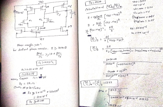
Design a two stage op amp with the following specifications Design Specifications Supply voltage ...
And b. slew lall unity-gain frequency amplifier. Specifications require that the gain vary no mor...
 4-47
ans:
a. 11.77Mhz
b. 40.21V/ms
c. yes
and b. slew lall unity-gain frequency amplifier. Specifications require that the gain vary no more than 2 dB from near The peak input signal is estimated as 0.8 V. Determine the minimum values of frequency and b. slew rate for the op-amp selected. c. Would the LM1182181 4-47. An inverting amplifier with a gain of -8 is to be designed for use in a s de to 1 MHz. a. unity-gain op-amp...
4-47
ans:
a. 11.77Mhz
b. 40.21V/ms
c. yes
and b. slew lall unity-gain frequency amplifier. Specifications require that the gain vary no more than 2 dB from near The peak input signal is estimated as 0.8 V. Determine the minimum values of frequency and b. slew rate for the op-amp selected. c. Would the LM1182181 4-47. An inverting amplifier with a gain of -8 is to be designed for use in a s de to 1 MHz. a. unity-gain op-amp...
1. Which of the following op amp IC design parameters limit the maximum gain? Select all...
1. Which of the following op amp IC design parameters limit the maximum gain? Select all that are true. -Signal frequency -DC power supply voltages -Rail voltages -Bandwidth -Resisters Rf and Ri 2. a. What is the TL081 op amp's Rail Voltage on each side? b. What is the TL081 op amp's Unity Gain Bandwidth? 3. If an op amp is considered to be "ideal", which of the following assumptions may be made? Select all that are true. -The op...
A. (10 pts) Implement the voltage amplifier shown below using an ideal op amp circuit. You have o...
 a. (10 pts) Implement the voltage amplifier shown below using an ideal op amp circuit. You have one op amp available for this circuit, and a range of resistors with values from 1 kΩ to 100 ka. Draw the schematic of your op amp circuit, labeling resistor values. Make sure the gain, input resistance, and output resistance of your circuit matches the model in the schematic. R=012 *100v, RL 100 b. (5 pts) Your amplifier circuit should have a frequency...
sedra smith book 7th edition chapter name is operational amplifier. question 12.1 to 12.10 I need...
 sedra smith book 7th edition chapter name is operational
amplifier. question 12.1 to 12.10 I need all solution with good
hand writing.
Problems 1075 Transistor Q3 WIL (um/um) 36/0.3 36/0.3 6/0.3 6/0.3 30/0.3 W/0.3 45/0.3 6/0.3 and A, if all devices are 0.3 m long, Q and Q2 are operated at overdrive voltages of 0.15-V magnitude, and Q is operated at Voy 0.2 V. Also, determine the op-amp output resistance 100 k2, C0.1 pF, G = 2 mA/V, R, =...
sedra smith book 7th edition chapter name is operational
amplifier. question 12.1 to 12.10 I need all solution with good
hand writing.
Problems 1075 Transistor Q3 WIL (um/um) 36/0.3 36/0.3 6/0.3 6/0.3 30/0.3 W/0.3 45/0.3 6/0.3 and A, if all devices are 0.3 m long, Q and Q2 are operated at overdrive voltages of 0.15-V magnitude, and Q is operated at Voy 0.2 V. Also, determine the op-amp output resistance 100 k2, C0.1 pF, G = 2 mA/V, R, =...
Vo-stage CMOS op amp of the type of 3 has C, = 2 pF and is fabricated in a rocess characterized b...
 For good rating provide correct and full solution
vo-stage CMOS op amp of the type of 3 has C, = 2 pF and is fabricated in a rocess characterized by k- 65 0.02 V and f, , and λ,-0.05 v-1. If SR = 40 V/μs 25 MHz, find the bias current /ss of the SC input pair, the overdrive voltage Voy and the of the individual SC transistors, and the Ist-stage de gain a,o REF 4 FIGURE 5.13 Two-stage CMOS...
For good rating provide correct and full solution
vo-stage CMOS op amp of the type of 3 has C, = 2 pF and is fabricated in a rocess characterized by k- 65 0.02 V and f, , and λ,-0.05 v-1. If SR = 40 V/μs 25 MHz, find the bias current /ss of the SC input pair, the overdrive voltage Voy and the of the individual SC transistors, and the Ist-stage de gain a,o REF 4 FIGURE 5.13 Two-stage CMOS...
4. A sinusoidal signal was used as the input to the inverting amplifier below. The op...
 4. A sinusoidal signal was used as the input to the inverting amplifier below. The op amp is ideal except for its open-loop gain. It has an open loop de gain (Ao) of 100dB and a unity-gain bandwidth (f) of 100 MHz. a) Find the transfer function, H(o), including the non-ideal open loop gain, A. b) Find the 3-dB frequency for the op amp, and sketch the |Al vs. frequency graph. Label the open loop de gain, 3-dB frequency, and...
D 8.106 The two-stage CMOS op amp in Fig. P8.106 is fabricated in a 0.18-um technology having 4 k...
 Please solve in details and in a clear way.
D 8.106 The two-stage CMOS op amp in Fig. P8.106 is fabricated in a 0.18-um technology having 4 kp tp (a) With A and B grounded, perform a dc design that will result in each of Q,, Q2, Qs, and Q, conducting a drain current of 100 uA and each of Q% and Q a current of 200 HA. Design so that all transistors operate at 0.2-V overdrive voltages. Specify the...
Please solve in details and in a clear way.
D 8.106 The two-stage CMOS op amp in Fig. P8.106 is fabricated in a 0.18-um technology having 4 kp tp (a) With A and B grounded, perform a dc design that will result in each of Q,, Q2, Qs, and Q, conducting a drain current of 100 uA and each of Q% and Q a current of 200 HA. Design so that all transistors operate at 0.2-V overdrive voltages. Specify the...
Miller e Frequency response of eireuits and multiple-stage amplifiers (with feedback) (50) 4. (10...
 Miller e Frequency response of eireuits and multiple-stage amplifiers (with feedback) (50) 4. (10) In the following amplifier circuit, the voltage source output resistance R,-2 k2, the op- amp can be considered as an ideal one except that it has a finite open-loop gain of 60 dB and an intrinsic input capacitance of Cn 20 pF. It's connected as an inverting amplifier. a) What frequency characteristic does this circuit have (HP or LP)? b) Design Ce so that the circuit...
Denve faih exmession VI + GIven the llowis Op Auf. en SKetch and abel axis tue...
 Denve faih exmession VI + GIven the llowis Op Auf. en SKetch and abel axis tue Picture" G Bu rAPh db 2.1 Model Parameters for the LM741 and the OPA300 Opamp amp Model "LM741" Library "LM 2 x 10⁵ 2 x 10⁶ Open-loop gain Input resistance Output resistance Positive voltage swing Negative voltage swing Input offset voltage Input bias current 75 21 -21 V 50 V 0.001 8 x 10⁻⁸ A 2x 10⁻⁸ 5 x 10⁵ 1.5 x 10⁶ 4.5x...
ELEC324/624 2018 Page 4 i) (2 marks) The open-loop frequency response of the LM748 op-amp is...
 ELEC324/624 2018 Page 4 i) (2 marks) The open-loop frequency response of the LM748 op-amp is shown in the figure be for two different values of the external compensating capacitor, Ci.If provides unity-gain compensation, determine the capacitance the op-amp for a closed-loop gain of 3 dB. C-30 pF required to compensat Open Loop Frequency Response 120 100 80 40 20 -20 FREQUENCY(Hx) j) (2 marks) Describe how delay in the loop of any feedback control system can seriously compromise the...
 4-47
ans:
a. 11.77Mhz
b. 40.21V/ms
c. yes
and b. slew lall unity-gain frequency amplifier. Specifications require that the gain vary no more than 2 dB from near The peak input signal is estimated as 0.8 V. Determine the minimum values of frequency and b. slew rate for the op-amp selected. c. Would the LM1182181 4-47. An inverting amplifier with a gain of -8 is to be designed for use in a s de to 1 MHz. a. unity-gain op-amp...
4-47
ans:
a. 11.77Mhz
b. 40.21V/ms
c. yes
and b. slew lall unity-gain frequency amplifier. Specifications require that the gain vary no more than 2 dB from near The peak input signal is estimated as 0.8 V. Determine the minimum values of frequency and b. slew rate for the op-amp selected. c. Would the LM1182181 4-47. An inverting amplifier with a gain of -8 is to be designed for use in a s de to 1 MHz. a. unity-gain op-amp...
 a. (10 pts) Implement the voltage amplifier shown below using an ideal op amp circuit. You have one op amp available for this circuit, and a range of resistors with values from 1 kΩ to 100 ka. Draw the schematic of your op amp circuit, labeling resistor values. Make sure the gain, input resistance, and output resistance of your circuit matches the model in the schematic. R=012 *100v, RL 100 b. (5 pts) Your amplifier circuit should have a frequency...
 sedra smith book 7th edition chapter name is operational
amplifier. question 12.1 to 12.10 I need all solution with good
hand writing.
Problems 1075 Transistor Q3 WIL (um/um) 36/0.3 36/0.3 6/0.3 6/0.3 30/0.3 W/0.3 45/0.3 6/0.3 and A, if all devices are 0.3 m long, Q and Q2 are operated at overdrive voltages of 0.15-V magnitude, and Q is operated at Voy 0.2 V. Also, determine the op-amp output resistance 100 k2, C0.1 pF, G = 2 mA/V, R, =...
sedra smith book 7th edition chapter name is operational
amplifier. question 12.1 to 12.10 I need all solution with good
hand writing.
Problems 1075 Transistor Q3 WIL (um/um) 36/0.3 36/0.3 6/0.3 6/0.3 30/0.3 W/0.3 45/0.3 6/0.3 and A, if all devices are 0.3 m long, Q and Q2 are operated at overdrive voltages of 0.15-V magnitude, and Q is operated at Voy 0.2 V. Also, determine the op-amp output resistance 100 k2, C0.1 pF, G = 2 mA/V, R, =...
 For good rating provide correct and full solution
vo-stage CMOS op amp of the type of 3 has C, = 2 pF and is fabricated in a rocess characterized by k- 65 0.02 V and f, , and λ,-0.05 v-1. If SR = 40 V/μs 25 MHz, find the bias current /ss of the SC input pair, the overdrive voltage Voy and the of the individual SC transistors, and the Ist-stage de gain a,o REF 4 FIGURE 5.13 Two-stage CMOS...
For good rating provide correct and full solution
vo-stage CMOS op amp of the type of 3 has C, = 2 pF and is fabricated in a rocess characterized by k- 65 0.02 V and f, , and λ,-0.05 v-1. If SR = 40 V/μs 25 MHz, find the bias current /ss of the SC input pair, the overdrive voltage Voy and the of the individual SC transistors, and the Ist-stage de gain a,o REF 4 FIGURE 5.13 Two-stage CMOS...
 4. A sinusoidal signal was used as the input to the inverting amplifier below. The op amp is ideal except for its open-loop gain. It has an open loop de gain (Ao) of 100dB and a unity-gain bandwidth (f) of 100 MHz. a) Find the transfer function, H(o), including the non-ideal open loop gain, A. b) Find the 3-dB frequency for the op amp, and sketch the |Al vs. frequency graph. Label the open loop de gain, 3-dB frequency, and...
 Please solve in details and in a clear way.
D 8.106 The two-stage CMOS op amp in Fig. P8.106 is fabricated in a 0.18-um technology having 4 kp tp (a) With A and B grounded, perform a dc design that will result in each of Q,, Q2, Qs, and Q, conducting a drain current of 100 uA and each of Q% and Q a current of 200 HA. Design so that all transistors operate at 0.2-V overdrive voltages. Specify the...
Please solve in details and in a clear way.
D 8.106 The two-stage CMOS op amp in Fig. P8.106 is fabricated in a 0.18-um technology having 4 kp tp (a) With A and B grounded, perform a dc design that will result in each of Q,, Q2, Qs, and Q, conducting a drain current of 100 uA and each of Q% and Q a current of 200 HA. Design so that all transistors operate at 0.2-V overdrive voltages. Specify the...
 Miller e Frequency response of eireuits and multiple-stage amplifiers (with feedback) (50) 4. (10) In the following amplifier circuit, the voltage source output resistance R,-2 k2, the op- amp can be considered as an ideal one except that it has a finite open-loop gain of 60 dB and an intrinsic input capacitance of Cn 20 pF. It's connected as an inverting amplifier. a) What frequency characteristic does this circuit have (HP or LP)? b) Design Ce so that the circuit...
 Denve faih exmession VI + GIven the llowis Op Auf. en SKetch and abel axis tue Picture" G Bu rAPh db 2.1 Model Parameters for the LM741 and the OPA300 Opamp amp Model "LM741" Library "LM 2 x 10⁵ 2 x 10⁶ Open-loop gain Input resistance Output resistance Positive voltage swing Negative voltage swing Input offset voltage Input bias current 75 21 -21 V 50 V 0.001 8 x 10⁻⁸ A 2x 10⁻⁸ 5 x 10⁵ 1.5 x 10⁶ 4.5x...
 ELEC324/624 2018 Page 4 i) (2 marks) The open-loop frequency response of the LM748 op-amp is shown in the figure be for two different values of the external compensating capacitor, Ci.If provides unity-gain compensation, determine the capacitance the op-amp for a closed-loop gain of 3 dB. C-30 pF required to compensat Open Loop Frequency Response 120 100 80 40 20 -20 FREQUENCY(Hx) j) (2 marks) Describe how delay in the loop of any feedback control system can seriously compromise the...
Most questions answered within 3 hours.
-
The number of major faults on a randomly chosen 1 km stretch of
highway has a...
asked 2 minutes ago -
Consider the competitive environment of Starbuck's, Progressive
Insurance, a manufacturing firm with low turnover, or a...
asked 49 minutes ago -
3. Gains from trade
Consider two neighbouring island countries called Euphoria and
Contente. They each have...
asked 2 hours ago -
A business executive has the option to invest money in two
plans: Plan A guarantees that...
asked 5 hours ago -
Hello, can someone please help me answer this question?
How much heat is absorbed by a...
asked 5 hours ago -
. A marketing researcher conducted a survey of 25 shoppers
randomly selected at the local mall...
asked 5 hours ago -
Create an comprehensive response to the
following:
Antimicrobial agents work on a multitude of microbes (bacteria,...
asked 5 hours ago -
6.13 LAB: Step counter. Section 6.3.
A pedometer treats walking 2,000 steps as walking 1 mile....
asked 5 hours ago -
(14.2) A block of mass m = 10 kg riding on a frictionless
horizontal plane is...
asked 5 hours ago -
Use any search engine to search for articles about Starbucks
partnership with Tata Companies in India...
asked 5 hours ago -
Let’s say that for some reason Bank Excess Reserves suddenly
increase sharply. What effect would this...
asked 5 hours ago -
Given:
Curent Assets: $600,000
Total Assets: $2,600,000
Current Liabilities: $500,000
Total Liabilities: $1,700,000
What is the...
asked 5 hours ago