
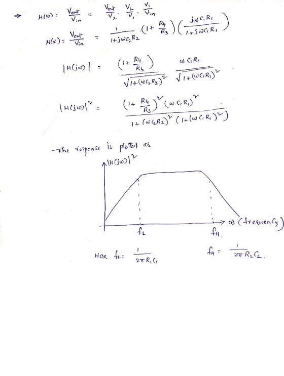
Homework Answers
Solution:
1) The first stage is a high pass filter circuit because at low frequency capacitor is open and does not allow the input and at high frequency capacitor is shorted and output is equal to input. It passes high frequency signals and attenuates low frequency signals.
Second stage is a DC amplifier with gain is equal to (1+R4/R3)
The third stage is a low pass filter circuit because at high frequency capacitor is open and allow the input and at low frequency capacitor is shorted and output is equal to zero. It passes low frequency signals and attenuates high frequency signals.
2) The total response is band pass response that will allow only signal frequencies between higher cutoff frequency fH and lower cutoff frequency fL.
3) Transfer function of each stage is found as,
Let output of first stage is taken as V1.
By voltage divider rule,
Capacitive reactance = Xc = 1/jwC1


Second stage, the transfer function is given by,
Let V2 be output voltage of second stage, and assume that op-amp is assumed to be ideal,

Transfer function of third stage is found as,
By voltage divider rule,
Capacitive reactance = Xc = 1/jwC2


4) The magnitude of the transfer function is given by,
Add Answer to:
Problem #1 (100pts) Consider the circuit shown in the Figure of three simpler circuits (stages). 1) Without solving...
Problem 4: For the following RLC circuit, R-1.01 kQ, 100 mH and C-0.1 μF. 1. Find...
 Problem 4: For the following RLC circuit, R-1.01 kQ, 100 mH and C-0.1 μF. 1. Find the transfer function H(jo) = Vo(jo)Vi(jo) 2. Find the gain of the transfer function | H(o) 3. Determin 4. Find the phase Ф(c) of the transfer function 5. Find Vo(t) if Vi(t) 100 cos(102 t) +60 cos (101 t) + 10 cos(106t) e the type of the filter. b) c) RVout Lo VoutVin Vin Vin Vin Vout Vout
QUESTION #2 PLEASE 1. Derive the transfer function for the circuit shown below. Plot H(s) versus...
 QUESTION #2 PLEASE
1. Derive the transfer function for the circuit shown below. Plot H(s) versus frequency in Hertz, on a semilog scale. Ri 11.3 k Ri 22.6 k R R = 68.1 kN R3 C C 0.01 uF R2 Vout(s) Vin(s) C2 10 (s+5) H(s) = (s+100)(s5000) , (a) draw the magnitude Bode plot 2. For the transfer function and find the approximate maximum value of (H(jw) in dB, (b) find the value of w where 1 for w>5...
QUESTION #2 PLEASE
1. Derive the transfer function for the circuit shown below. Plot H(s) versus frequency in Hertz, on a semilog scale. Ri 11.3 k Ri 22.6 k R R = 68.1 kN R3 C C 0.01 uF R2 Vout(s) Vin(s) C2 10 (s+5) H(s) = (s+100)(s5000) , (a) draw the magnitude Bode plot 2. For the transfer function and find the approximate maximum value of (H(jw) in dB, (b) find the value of w where 1 for w>5...
who can solve this problem? thanks Problem 3: Chain rule and circuit design Consider the circuit in the below figure...
 who can solve this problem? thanks
Problem 3: Chain rule and circuit design Consider the circuit in the below figure. You can as me zero initial conditions. t WW-어 2R L stage 1 stage 3 stage 4 stage 2 Part I: Redraw the above circuit in the s-domain and compute the transfer functions Ti(s), T(s). Tfs), Tds) of each one stages Part II: Somebody with a rusty recollection of linear circuits analyzed the above circuit and concluded that the transfer...
who can solve this problem? thanks
Problem 3: Chain rule and circuit design Consider the circuit in the below figure. You can as me zero initial conditions. t WW-어 2R L stage 1 stage 3 stage 4 stage 2 Part I: Redraw the above circuit in the s-domain and compute the transfer functions Ti(s), T(s). Tfs), Tds) of each one stages Part II: Somebody with a rusty recollection of linear circuits analyzed the above circuit and concluded that the transfer...
1. Find the transfer function Voda)/Vin(a) for the circuit shown in Figure 1 of the lab (where co...
 Please answer number 1
1. Find the transfer function Voda)/Vin(a) for the circuit shown in Figure 1 of the lab (where complex frequency variable s jo can be substituted for ease of analysis.) Calculate values for R and C such that the phase shift between the output and input is zero for an input frequency of 10kHz. What is the amplitude ratio (gain) of the output to the input at this frequency. 2. The RC network in figure 3 of...
Please answer number 1
1. Find the transfer function Voda)/Vin(a) for the circuit shown in Figure 1 of the lab (where complex frequency variable s jo can be substituted for ease of analysis.) Calculate values for R and C such that the phase shift between the output and input is zero for an input frequency of 10kHz. What is the amplitude ratio (gain) of the output to the input at this frequency. 2. The RC network in figure 3 of...
Problem 1: /25 For the circuit shown below, use frequency-domain circuit analysis techniques to determine (a)...
 Problem 1: /25 For the circuit shown below, use frequency-domain circuit analysis techniques to determine (a) the voltage transfer function Ho) of the circuit; (b) the magnitude response H(o) of the circuit; and (c) the phase response (0) of the circuit. (d) Based on the results of parts (a) - (c), identify the type of filter circuit shown. R + Vin(t) llll L Vout(t)
5. [RC Circuits] Consider the circuit shown in Figure 5 attached. As shown, the switch is...
 5. [RC Circuits] Consider the circuit shown in Figure 5 attached. As shown, the switch is in position "A" for t < 0, and the circuit has been at rest for a long time. At time t = 0, the switch opens and the capacitor starts to drain across the resistor. (a) When the switch is closed and there is only a direct current (DC) source, the capacitor acts like an open circuit. Find the constant voltage across the capacitor...
PROBLEM #1: The circuit shown in Figure P4.4 consists of the cascade connection of three sections....
 PROBLEM #1: The circuit shown in Figure P4.4 consists of the cascade connection of three sections. In the total circuit all C's are equal and all R's are equal. (a) Let V= 0 and find the transfer function T(s) = (8) (b) Connect node 0 to node 2 such that V. =V,, and determine the transfer function under this condition. V (S) linn -- R +013 + RS FIGURE P4.4
Prelab Preparation: For the RC circuit shown in Figure 1, derive the modeling equation relating the output volta ge...
 Prelab Preparation: For the RC circuit shown in Figure 1, derive the modeling equation relating the output volta ge Vout to the input voltage vin. What is the transfer function? What is the time constant of the system? Vout Figure 1: RC Circuit What is the analytical step response solution in terms of vin, Rand C? For assumed values of R 1 K, and C 6.8 uF, perform a simulation using Matlab/Simulink assuming an input square wave signal of 5Vpp,...
Consider the filter circuit (Figure 1) with R=500 N and C ==uF. Learning Goal: To understand...
 Consider the filter circuit (Figure 1) with R=500 N and C ==uF. Learning Goal: To understand how to find the transfer function of a filter circuit and to be able to draw the asymptotes of the Bode magnitude and phase diagrams Bode plots are used to display the amplitude and phase of a transfer function. The amplitude is typically displayed by showing the magnitude of the transfer function on the vertical axis and the frequency on the horizontal axis using...
Problem 1 (25 Pts) Consider the OP amp circuit shown below with R = 100kN and...
 Problem 1 (25 Pts) Consider the OP amp circuit shown below with R = 100kN and C = 1(10): Parta) 10 pts Find the complex transfer function for the circuit in terms of frequency f(Hz). Part b) 5 pts Compute the gain of at as a function of frequency f(Hz). Parte) 10 pts Compute the corresponding gains at 100, 1000, 10000 Hz. R 3R 5R Vå w V
 Problem 4: For the following RLC circuit, R-1.01 kQ, 100 mH and C-0.1 μF. 1. Find the transfer function H(jo) = Vo(jo)Vi(jo) 2. Find the gain of the transfer function | H(o) 3. Determin 4. Find the phase Ф(c) of the transfer function 5. Find Vo(t) if Vi(t) 100 cos(102 t) +60 cos (101 t) + 10 cos(106t) e the type of the filter. b) c) RVout Lo VoutVin Vin Vin Vin Vout Vout
 QUESTION #2 PLEASE
1. Derive the transfer function for the circuit shown below. Plot H(s) versus frequency in Hertz, on a semilog scale. Ri 11.3 k Ri 22.6 k R R = 68.1 kN R3 C C 0.01 uF R2 Vout(s) Vin(s) C2 10 (s+5) H(s) = (s+100)(s5000) , (a) draw the magnitude Bode plot 2. For the transfer function and find the approximate maximum value of (H(jw) in dB, (b) find the value of w where 1 for w>5...
QUESTION #2 PLEASE
1. Derive the transfer function for the circuit shown below. Plot H(s) versus frequency in Hertz, on a semilog scale. Ri 11.3 k Ri 22.6 k R R = 68.1 kN R3 C C 0.01 uF R2 Vout(s) Vin(s) C2 10 (s+5) H(s) = (s+100)(s5000) , (a) draw the magnitude Bode plot 2. For the transfer function and find the approximate maximum value of (H(jw) in dB, (b) find the value of w where 1 for w>5...
 who can solve this problem? thanks
Problem 3: Chain rule and circuit design Consider the circuit in the below figure. You can as me zero initial conditions. t WW-어 2R L stage 1 stage 3 stage 4 stage 2 Part I: Redraw the above circuit in the s-domain and compute the transfer functions Ti(s), T(s). Tfs), Tds) of each one stages Part II: Somebody with a rusty recollection of linear circuits analyzed the above circuit and concluded that the transfer...
who can solve this problem? thanks
Problem 3: Chain rule and circuit design Consider the circuit in the below figure. You can as me zero initial conditions. t WW-어 2R L stage 1 stage 3 stage 4 stage 2 Part I: Redraw the above circuit in the s-domain and compute the transfer functions Ti(s), T(s). Tfs), Tds) of each one stages Part II: Somebody with a rusty recollection of linear circuits analyzed the above circuit and concluded that the transfer...
 Please answer number 1
1. Find the transfer function Voda)/Vin(a) for the circuit shown in Figure 1 of the lab (where complex frequency variable s jo can be substituted for ease of analysis.) Calculate values for R and C such that the phase shift between the output and input is zero for an input frequency of 10kHz. What is the amplitude ratio (gain) of the output to the input at this frequency. 2. The RC network in figure 3 of...
Please answer number 1
1. Find the transfer function Voda)/Vin(a) for the circuit shown in Figure 1 of the lab (where complex frequency variable s jo can be substituted for ease of analysis.) Calculate values for R and C such that the phase shift between the output and input is zero for an input frequency of 10kHz. What is the amplitude ratio (gain) of the output to the input at this frequency. 2. The RC network in figure 3 of...
 Problem 1: /25 For the circuit shown below, use frequency-domain circuit analysis techniques to determine (a) the voltage transfer function Ho) of the circuit; (b) the magnitude response H(o) of the circuit; and (c) the phase response (0) of the circuit. (d) Based on the results of parts (a) - (c), identify the type of filter circuit shown. R + Vin(t) llll L Vout(t)
 5. [RC Circuits] Consider the circuit shown in Figure 5 attached. As shown, the switch is in position "A" for t < 0, and the circuit has been at rest for a long time. At time t = 0, the switch opens and the capacitor starts to drain across the resistor. (a) When the switch is closed and there is only a direct current (DC) source, the capacitor acts like an open circuit. Find the constant voltage across the capacitor...
 PROBLEM #1: The circuit shown in Figure P4.4 consists of the cascade connection of three sections. In the total circuit all C's are equal and all R's are equal. (a) Let V= 0 and find the transfer function T(s) = (8) (b) Connect node 0 to node 2 such that V. =V,, and determine the transfer function under this condition. V (S) linn -- R +013 + RS FIGURE P4.4
 Prelab Preparation: For the RC circuit shown in Figure 1, derive the modeling equation relating the output volta ge Vout to the input voltage vin. What is the transfer function? What is the time constant of the system? Vout Figure 1: RC Circuit What is the analytical step response solution in terms of vin, Rand C? For assumed values of R 1 K, and C 6.8 uF, perform a simulation using Matlab/Simulink assuming an input square wave signal of 5Vpp,...
 Consider the filter circuit (Figure 1) with R=500 N and C ==uF. Learning Goal: To understand how to find the transfer function of a filter circuit and to be able to draw the asymptotes of the Bode magnitude and phase diagrams Bode plots are used to display the amplitude and phase of a transfer function. The amplitude is typically displayed by showing the magnitude of the transfer function on the vertical axis and the frequency on the horizontal axis using...
 Problem 1 (25 Pts) Consider the OP amp circuit shown below with R = 100kN and C = 1(10): Parta) 10 pts Find the complex transfer function for the circuit in terms of frequency f(Hz). Part b) 5 pts Compute the gain of at as a function of frequency f(Hz). Parte) 10 pts Compute the corresponding gains at 100, 1000, 10000 Hz. R 3R 5R Vå w V
Most questions answered within 3 hours.
-
A 0.25μF capacitor is charged to 50 V . It is then connected in
series with...
asked 13 minutes ago -
Calculate the current, I, through the batteries for:
- a 2-bulb parallel circuit
- How does...
asked 15 minutes ago -
Choose the sentence that uses correct punctuation.
1a. The prefatory parts of a report include the...
asked 21 minutes ago -
For the element arsenic, which one of the following sets of
quantum numbers could not apply...
asked 30 minutes ago -
Compare and contrast the architectures of 3 types of ADCs:
Flash, SAR, and pipelined. Use the...
asked 31 minutes ago -
Given P(A) = 0.40, P(B) = 0.50, P(A ∩ B) = 0.15. Which of the
following...
asked 36 minutes ago -
Explain changes in workforce participation for women with
children. What legislation exists related to work and...
asked 38 minutes ago -
How high must a pointed arch be if it is to span a
space 4.2 m...
asked 43 minutes ago -
A housepainter who weighs 750 N stands 0.6 m from one end of a
2.0 m...
asked 45 minutes ago -
Implement Singly Linked List detectLoop in Java.
It would check whether the linked list contains a...
asked 48 minutes ago -
A small mailbag is released from a helicopter that is descending
steadily at 2.10 m/s.
After...
asked 49 minutes ago -
Write a C – program that calls a user-defined function from
within main() that determines the...
asked 52 minutes ago