
Homework Answers
 kindly upvote if it's helpful
for you .
kindly upvote if it's helpful
for you .
Add Answer to:
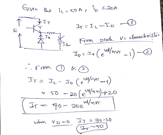
Please Show Working Q2- The load current i, in the following circuit is 50 A constant. The diode has a maximum reverse...
A MOSFET and diode is used in a circuit shown in figure. The operating conditions are...
A MOSFET and diode is used in a circuit shown in figure. The operating conditions are as follows: Input Voltage = VIN = 42 V, Io = 5A. Switching frequency fs = 400 kHz, Duty-cycle = D = 0.3. Diode Forward Voltage drop = 0.7V. Diode Peak Reverse Recovery Current = IRRM = 2.5 A. ON-state resistance of the MOSFET is RDS (on) = 25 mΩ. VGG as a step voltage between 0V and 10 V. MOSFET timings – Td...
please help Question 1 Consider the following circuit, where the reverse saturation current (Is) is the...
 please help
Question 1 Consider the following circuit, where the reverse saturation current (Is) is the same for each diode. D2 o Vo Di Vi WWW R 32 23 a. b. Determine an algebraic expression for V1, for a given Vo, and Is. Given an Is of 40 FA and R1 = 3.3 kl , determine the Vi that produces an output voltage (V.) of 0.625 V. C. Recalculate question-b if Is were to be a thousand times greater at...
please help
Question 1 Consider the following circuit, where the reverse saturation current (Is) is the same for each diode. D2 o Vo Di Vi WWW R 32 23 a. b. Determine an algebraic expression for V1, for a given Vo, and Is. Given an Is of 40 FA and R1 = 3.3 kl , determine the Vi that produces an output voltage (V.) of 0.625 V. C. Recalculate question-b if Is were to be a thousand times greater at...
To design a high efficiency d.c., to d.c power converter with the given specifications min 10V max 15V nominal (regulated) 8V Input voltage: Output voltage: Nominal load current: 4A Inductor current...
 To design a high efficiency d.c., to d.c power converter with the given specifications min 10V max 15V nominal (regulated) 8V Input voltage: Output voltage: Nominal load current: 4A Inductor current ripple: 0.1A max Switching frequency: 30 kHz Output voltage ripple: 20 mV Define a suitable power circuit topology to meet the above specification? Sketch a circuit diagram of the chosen power circuit topology (a) Define the minimum and maximum duty cycles assuming that the control circuit keeps the output...
Question 1 220 Vrms 50 Hz 10:1 CR Figure 1 Figure 1 shows the circuit diagram...
 Question 1 220 Vrms 50 Hz 10:1 CR Figure 1 Figure 1 shows the circuit diagram for a simple d.c. power supply. a. Identify the type of rectifier circuit represented in figure I and explain the operation of the circuit with reference to the function of each component within the circuit. b. Sketch to scale the voltage across R as a function of time showing its relationship to the secondary voltage from the transformer. Question 2 A 5.0V stabilized power...
Problems,,,,,
 1 2
+
–
i(t)
C R
L
iT i(t)
iD
+
–
L C R
1. Analysis and design of a buck-boost converter: A buck-boost converter is illustrated in Fig. 1(a),
and a practical implementation using a transistor and diode is shown in Fig. 1(b).
+
(a)
Vg
v
Figure 1 Buck–boost converter
of Problem 1: (a) ideal converter
circuit, (b) implementation using
MOSFET and diode.
–
Q1
D1
(b) +
Vg
v
Page 2
iL
(t) + vL...
1 2
+
–
i(t)
C R
L
iT i(t)
iD
+
–
L C R
1. Analysis and design of a buck-boost converter: A buck-boost converter is illustrated in Fig. 1(a),
and a practical implementation using a transistor and diode is shown in Fig. 1(b).
+
(a)
Vg
v
Figure 1 Buck–boost converter
of Problem 1: (a) ideal converter
circuit, (b) implementation using
MOSFET and diode.
–
Q1
D1
(b) +
Vg
v
Page 2
iL
(t) + vL...
a9a resistive load. Inductor 3-(35 pts) Design a converter that has an input voltage of 24 V DC and supplies 18 V DC to current is desired to be continuous and must not change more than 30 % of i...
 a9a resistive load. Inductor 3-(35 pts) Design a converter that has an input voltage of 24 V DC and supplies 18 V DC to current is desired to be continuous and must not change more than 30 % of its average value voltage ripple must be lower than 2 %. Switching frequency is 10 kHz. a) Draw the circuit diagram. Calculate the duty ratio. Calculate values for 2 desired conditions of the inductor current and determine the value of the...
****Please ALL answers questions with complete steps.**** 1. Analysis and design of a buck-boost converter. A...
 ****Please ALL answers questions with complete
steps.****
1. Analysis and design of a buck-boost converter. A buck-boost converter is illustrated below. + licit) + reee c= R { v(t) A practical implementation using a MOSFET and diode is illustrated below. D + Voi(t) – H + iqi(t) IT int) lic(t) iz(t) + LE vi(t) c R v(t) For this problem, you must employ the methods of inductor volt-second balance, capacitor charge balance, and the small ripple approximation as discussed in...
****Please ALL answers questions with complete
steps.****
1. Analysis and design of a buck-boost converter. A buck-boost converter is illustrated below. + licit) + reee c= R { v(t) A practical implementation using a MOSFET and diode is illustrated below. D + Voi(t) – H + iqi(t) IT int) lic(t) iz(t) + LE vi(t) c R v(t) For this problem, you must employ the methods of inductor volt-second balance, capacitor charge balance, and the small ripple approximation as discussed in...
A common source amplifier circuit based on a single n-channel MOSFET is shown in Figure 4b. Assume that the transconductance gm-60 mS (equivalent to mA/ V) and drain source resistance, os,...
 A common source amplifier circuit based on a single n-channel MOSFET is shown in Figure 4b. Assume that the transconductance gm-60 mS (equivalent to mA/ V) and drain source resistance, os, is so large it may be neglected. 0) Calculate the open circuit voltage gain Av Yout/ Vis. i) The amplifier has a load of 10 k2. Determine the current gain Va. = 12 V 150k 4k3 Vout Vin 200k GND = 0 V Figure 4b a) State the name...
O bructe CONFIDENTIAL 2 limitatio of Flyb Q2 (a) With the aid of respective topology, point...
 O bructe CONFIDENTIAL 2 limitatio of Flyb Q2 (a) With the aid of respective topology, point out three (3) basic de-de converters ( 3 marks) (b) Discuss the energy transfer in on each circuit by refering the circuits drawn in Q2(a) (3 marks) (c) Design a boost converter for continuous inductor current and an output nipple voltage of less than 1% that will have an output of 30 V from a 12 V source, Assume the load resistance of 50...
 please help
Question 1 Consider the following circuit, where the reverse saturation current (Is) is the same for each diode. D2 o Vo Di Vi WWW R 32 23 a. b. Determine an algebraic expression for V1, for a given Vo, and Is. Given an Is of 40 FA and R1 = 3.3 kl , determine the Vi that produces an output voltage (V.) of 0.625 V. C. Recalculate question-b if Is were to be a thousand times greater at...
please help
Question 1 Consider the following circuit, where the reverse saturation current (Is) is the same for each diode. D2 o Vo Di Vi WWW R 32 23 a. b. Determine an algebraic expression for V1, for a given Vo, and Is. Given an Is of 40 FA and R1 = 3.3 kl , determine the Vi that produces an output voltage (V.) of 0.625 V. C. Recalculate question-b if Is were to be a thousand times greater at...
 To design a high efficiency d.c., to d.c power converter with the given specifications min 10V max 15V nominal (regulated) 8V Input voltage: Output voltage: Nominal load current: 4A Inductor current ripple: 0.1A max Switching frequency: 30 kHz Output voltage ripple: 20 mV Define a suitable power circuit topology to meet the above specification? Sketch a circuit diagram of the chosen power circuit topology (a) Define the minimum and maximum duty cycles assuming that the control circuit keeps the output...
 Question 1 220 Vrms 50 Hz 10:1 CR Figure 1 Figure 1 shows the circuit diagram for a simple d.c. power supply. a. Identify the type of rectifier circuit represented in figure I and explain the operation of the circuit with reference to the function of each component within the circuit. b. Sketch to scale the voltage across R as a function of time showing its relationship to the secondary voltage from the transformer. Question 2 A 5.0V stabilized power...
 a9a resistive load. Inductor 3-(35 pts) Design a converter that has an input voltage of 24 V DC and supplies 18 V DC to current is desired to be continuous and must not change more than 30 % of its average value voltage ripple must be lower than 2 %. Switching frequency is 10 kHz. a) Draw the circuit diagram. Calculate the duty ratio. Calculate values for 2 desired conditions of the inductor current and determine the value of the...
 ****Please ALL answers questions with complete
steps.****
1. Analysis and design of a buck-boost converter. A buck-boost converter is illustrated below. + licit) + reee c= R { v(t) A practical implementation using a MOSFET and diode is illustrated below. D + Voi(t) – H + iqi(t) IT int) lic(t) iz(t) + LE vi(t) c R v(t) For this problem, you must employ the methods of inductor volt-second balance, capacitor charge balance, and the small ripple approximation as discussed in...
****Please ALL answers questions with complete
steps.****
1. Analysis and design of a buck-boost converter. A buck-boost converter is illustrated below. + licit) + reee c= R { v(t) A practical implementation using a MOSFET and diode is illustrated below. D + Voi(t) – H + iqi(t) IT int) lic(t) iz(t) + LE vi(t) c R v(t) For this problem, you must employ the methods of inductor volt-second balance, capacitor charge balance, and the small ripple approximation as discussed in...
 A common source amplifier circuit based on a single n-channel MOSFET is shown in Figure 4b. Assume that the transconductance gm-60 mS (equivalent to mA/ V) and drain source resistance, os, is so large it may be neglected. 0) Calculate the open circuit voltage gain Av Yout/ Vis. i) The amplifier has a load of 10 k2. Determine the current gain Va. = 12 V 150k 4k3 Vout Vin 200k GND = 0 V Figure 4b a) State the name...
 O bructe CONFIDENTIAL 2 limitatio of Flyb Q2 (a) With the aid of respective topology, point out three (3) basic de-de converters ( 3 marks) (b) Discuss the energy transfer in on each circuit by refering the circuits drawn in Q2(a) (3 marks) (c) Design a boost converter for continuous inductor current and an output nipple voltage of less than 1% that will have an output of 30 V from a 12 V source, Assume the load resistance of 50...
 O bructe CONFIDENTIAL 2 limitatio of Flyb Q2 (a) With the aid of respective topology, point out three (3) basic de-de converters ( 3 marks) (b) Discuss the energy transfer in on each circuit by refering the circuits drawn in Q2(a) (3 marks) (c) Design a boost converter for continuous inductor current and an output nipple voltage of less than 1% that will have an output of 30 V from a 12 V source, Assume the load resistance of 50...
Most questions answered within 3 hours.
-
1.A solution has a pH of 5.5. What would be the color of the
solution if...
asked 28 seconds ago -
Adidas Runs Into Supply-Chain Problems in Crucial North
American Market
Shares fall amid concern the sporting-goods...
asked 35 seconds ago -
The physical plant at the main campus of a large state
university recieves daily requests to...
asked 39 minutes ago -
Determine the probability p(2) for a binomial
experiment with n=12 trials and the success probability
p=0.1....
asked 12 minutes ago -
What is the vapor pressure at 20 degrees C of an ideal solution
prepared by the...
asked 9 minutes ago -
You want to find the independent and dependent variables taken
from a sample of 30 dropouts....
asked 42 minutes ago -
. A light signal is traveling through a fiber. What is the delay
in the signal...
asked 31 minutes ago -
“Architects can have an important and direct impact on thermal
comfort and IAQ for improving design...
asked 15 minutes ago -
A 1.10 kg sample of a metal sample absorbs 43.5 kJ of heat,
resulting in a...
asked 39 minutes ago -
Many pharmaceutical compounds contain amine functional groups,
as they are adapted from amine-containing alkaloids. These drugs...
asked 19 minutes ago -
W Corporation uses the FIFO method of process costing. At the
beginning of the period, there...
asked 19 minutes ago -
what principal will have a maturity value of $61,500
at 6.5% in 17 months
asked 23 minutes ago