For the MOSFET circuit, 
Given 


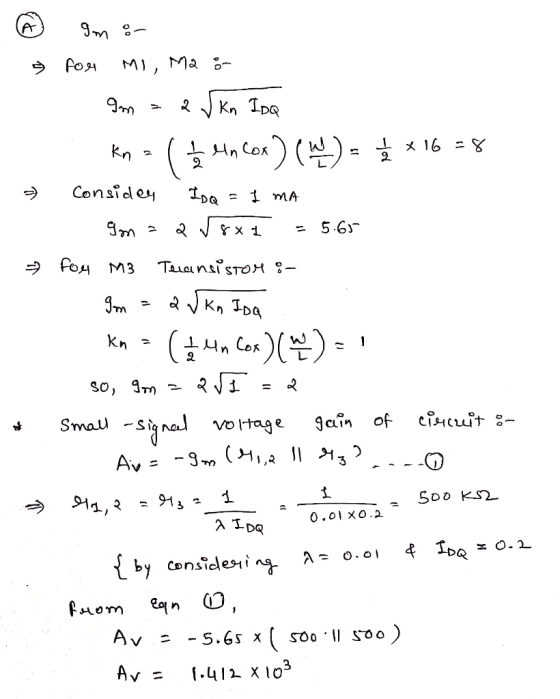
a) Find the transconductance of all 3 transistors (in terms of Io) and the small-signal voltage gain of the circuit. Assume all transistors are in saturation.
b) Find R1 (looking into the source of M1) and R2 (looking into the source of M2).

166 L
1 L
4n Cor = 1
Vpp R1 R2
Homework Answers
Add Answer to:
For the MOSFET circuit, . Given for M1 and M2, and for M3. (A/V2) for all transistors. a) Find the transconductanc...
For the MOSFET circuit, . Given for M1 and M2, and for M3. (A/V2) for all...
 For the MOSFET circuit,
.
Given
for M1 and M2, and
for M3.
(A/V2) for all transistors.
a) Find the transconductance of all 3 transistors (in terms of
Io) and the small-signal voltage gain of the circuit.
Assume all transistors are in saturation.
b) Find R1 (looking into the source of M1)
and R2 (looking into the source of M2).
8nCor 166 L 1 L 4n Cor = 1 Vpp R1 R2
For the MOSFET circuit,
.
Given
for M1 and M2, and
for M3.
(A/V2) for all transistors.
a) Find the transconductance of all 3 transistors (in terms of
Io) and the small-signal voltage gain of the circuit.
Assume all transistors are in saturation.
b) Find R1 (looking into the source of M1)
and R2 (looking into the source of M2).
8nCor 166 L 1 L 4n Cor = 1 Vpp R1 R2
Given β=16 for M1 and M2, and that β=1 for M3. a) Find the gm of...
 Given β=16 for M1 and M2, and that β=1 for
M3.
a) Find the gm of all 3 transistors (in terms of
Io) and the small-signal voltage gain of the circuit.
Assume all transistors are in saturation.
b) Find R1 (looking into the source of M1)
and R2 (looking into the source of M2).
Vpp R1 R2
Vpp R1 R2
Given β=16 for M1 and M2, and that β=1 for
M3.
a) Find the gm of all 3 transistors (in terms of
Io) and the small-signal voltage gain of the circuit.
Assume all transistors are in saturation.
b) Find R1 (looking into the source of M1)
and R2 (looking into the source of M2).
Vpp R1 R2
Vpp R1 R2
4) Consider the MOSFET differential amplifier shown below, with Io-2 mA, and RL- 10 kS2, Rss-100 ...
 4) Consider the MOSFET differential amplifier shown below, with Io-2 mA, and RL- 10 kS2, Rss-100 k2, VDD- +8V and Vss--8V. The NMOS transistors in the circuit are nominally identical, with kn 2 mA/V2, VTn 1.0 V and ro 100 k2. The PMoS transistors in the circuit are nominally identical, with kp 2 mA/V2, [VTpl 1.0 V and ro 100 kΩ M3 M4 0 M1 M2 a) First consider the DC bias point. Assuming that the current mirror requires at...
2. For the amplifiers below, not all the bias details are shown. For the circuit on the left, what is the small signal...
 2. For the amplifiers below, not all the bias details are shown. For the circuit on the left, what is the small signal resistance looking into the a. source of M2 (Ri2)? b. Using part a, Find the voltage gain at the drain of Mi, and the total gain at the output. For the circuit on the right, known as a cascode amplifier, find the voltage gain. c. Express your answers in terms of the transistors gm, and RD. Assume...
PROBLEM 4 (20 pts) IMPORTANT: Assume all transistors are in saturation. a) Find the small-signal DC...
 PROBLEM 4 (20 pts) IMPORTANT: Assume all transistors are in saturation. a) Find the small-signal DC gain of the amplifier circuit when the small-signal voltage ViN is applied to the gate of M1. Ignore the body effect for M1 and M2. b) Find the small-signal DC gain of the amplifier circuit when the small-signal voltage Vin is applied to the body of M1. In this case, a DC bias voltage (VB) is applied to the gate of M1. Ignore the...
Problem #1 (3 pts) Assuming that all transistors are saturated and operating in subthreshold. Assume identical...
 Problem #1 (3 pts) Assuming that all transistors are saturated and operating in subthreshold. Assume identical transistors. IB a) b) c) If V1-V2, what is 11, 12, and Vx? Draw the small signal equivalent circuit. If (in DC) V1 -V2, what is the small signal transconductance V2 is the input. Use the low-frequency small signal model with no capacitors and no Early effect. Include Vx M1 M3 M2 12 M4 0 . Assume that V1 is fixed and the body...
All nMOS transistors in the circuit shown are identical, have k' WIL 4 mA/V2 and operate...
 All nMOS transistors in the circuit shown are identical, have k' WIL 4 mA/V2 and operate in the active region lp 1/2k 'W/L(Vas-V)']. Knowing that the de voltage VD4 at the drain of Q4-2 V. Determine: 1. The value of the bias current lo 2. The value of Vov 3. The transconductance gm of Q1 and Q2 4. The voltage gain vo/v 5. The voltage gain when a source resistance R, 1K2 is added to the source of Qi and...
5) Consider the Cascode amplifier shown below. For the NMOS transistors, kn 0.2 mA/V2, Vr,-0.5 V,...
 5) Consider the Cascode amplifier shown below. For the NMOS transistors, kn 0.2 mA/V2, Vr,-0.5 V, (W/L)-(W/L)2-5. VDD-GV and IBIAs= 1.0 mA. a) Assuming λ-0 for all transistors, find the required DC gate- source voltages of M1 and M2 (VGsı and VGs2, respectively) BIAS VD out b) Again assuming 0 M2 for all transistors, what is the minimum DC value of VouT for which the amplifier works in high-gain regime? (W/L)2 in M1 For parts c)-f), Assume -0.01 for all...
3. In the circuit shown below, the differential pair (Mand M2) is biased with a current miror that consists of M3, M and Rref. The circuit parameters are: VDD-3 V, Rre/-15 ka, RD = 20 ka, and RL-40 k...
 3. In the circuit shown below, the differential pair (Mand M2) is biased with a current miror that consists of M3, M and Rref. The circuit parameters are: VDD-3 V, Rre/-15 ka, RD = 20 ka, and RL-40 kn. The transistors 25 M, and M, are identicalwith()M and M, are identical with (The oh M and M4 are identical with = ·The other transistor parameters are: indox-: 0.1 m1A/V2,VTN-0.5 V, γ-0 (body effect coefficient) and λ 0 (channel length modulation...
Assume 1 = 0, compute W/L of M1 in the circuit below such that the MOSFET...
 Assume 1 = 0, compute W/L of M1 in the circuit below such that the MOSFET operates at the edge of saturation knowing Vpp = 1.8 V T Rp 1k02 that H.Cox = 2004A/V2 and Vth=0.4V M1 1 V Select one: O a. 300 b. 33 O c. 30 O d. 330 e. None of these
 For the MOSFET circuit,
.
Given
for M1 and M2, and
for M3.
(A/V2) for all transistors.
a) Find the transconductance of all 3 transistors (in terms of
Io) and the small-signal voltage gain of the circuit.
Assume all transistors are in saturation.
b) Find R1 (looking into the source of M1)
and R2 (looking into the source of M2).
8nCor 166 L 1 L 4n Cor = 1 Vpp R1 R2
For the MOSFET circuit,
.
Given
for M1 and M2, and
for M3.
(A/V2) for all transistors.
a) Find the transconductance of all 3 transistors (in terms of
Io) and the small-signal voltage gain of the circuit.
Assume all transistors are in saturation.
b) Find R1 (looking into the source of M1)
and R2 (looking into the source of M2).
8nCor 166 L 1 L 4n Cor = 1 Vpp R1 R2
 Given β=16 for M1 and M2, and that β=1 for
M3.
a) Find the gm of all 3 transistors (in terms of
Io) and the small-signal voltage gain of the circuit.
Assume all transistors are in saturation.
b) Find R1 (looking into the source of M1)
and R2 (looking into the source of M2).
Vpp R1 R2
Vpp R1 R2
Given β=16 for M1 and M2, and that β=1 for
M3.
a) Find the gm of all 3 transistors (in terms of
Io) and the small-signal voltage gain of the circuit.
Assume all transistors are in saturation.
b) Find R1 (looking into the source of M1)
and R2 (looking into the source of M2).
Vpp R1 R2
Vpp R1 R2
 4) Consider the MOSFET differential amplifier shown below, with Io-2 mA, and RL- 10 kS2, Rss-100 k2, VDD- +8V and Vss--8V. The NMOS transistors in the circuit are nominally identical, with kn 2 mA/V2, VTn 1.0 V and ro 100 k2. The PMoS transistors in the circuit are nominally identical, with kp 2 mA/V2, [VTpl 1.0 V and ro 100 kΩ M3 M4 0 M1 M2 a) First consider the DC bias point. Assuming that the current mirror requires at...
 2. For the amplifiers below, not all the bias details are shown. For the circuit on the left, what is the small signal resistance looking into the a. source of M2 (Ri2)? b. Using part a, Find the voltage gain at the drain of Mi, and the total gain at the output. For the circuit on the right, known as a cascode amplifier, find the voltage gain. c. Express your answers in terms of the transistors gm, and RD. Assume...
 PROBLEM 4 (20 pts) IMPORTANT: Assume all transistors are in saturation. a) Find the small-signal DC gain of the amplifier circuit when the small-signal voltage ViN is applied to the gate of M1. Ignore the body effect for M1 and M2. b) Find the small-signal DC gain of the amplifier circuit when the small-signal voltage Vin is applied to the body of M1. In this case, a DC bias voltage (VB) is applied to the gate of M1. Ignore the...
 Problem #1 (3 pts) Assuming that all transistors are saturated and operating in subthreshold. Assume identical transistors. IB a) b) c) If V1-V2, what is 11, 12, and Vx? Draw the small signal equivalent circuit. If (in DC) V1 -V2, what is the small signal transconductance V2 is the input. Use the low-frequency small signal model with no capacitors and no Early effect. Include Vx M1 M3 M2 12 M4 0 . Assume that V1 is fixed and the body...
 All nMOS transistors in the circuit shown are identical, have k' WIL 4 mA/V2 and operate in the active region lp 1/2k 'W/L(Vas-V)']. Knowing that the de voltage VD4 at the drain of Q4-2 V. Determine: 1. The value of the bias current lo 2. The value of Vov 3. The transconductance gm of Q1 and Q2 4. The voltage gain vo/v 5. The voltage gain when a source resistance R, 1K2 is added to the source of Qi and...
 5) Consider the Cascode amplifier shown below. For the NMOS transistors, kn 0.2 mA/V2, Vr,-0.5 V, (W/L)-(W/L)2-5. VDD-GV and IBIAs= 1.0 mA. a) Assuming λ-0 for all transistors, find the required DC gate- source voltages of M1 and M2 (VGsı and VGs2, respectively) BIAS VD out b) Again assuming 0 M2 for all transistors, what is the minimum DC value of VouT for which the amplifier works in high-gain regime? (W/L)2 in M1 For parts c)-f), Assume -0.01 for all...
 3. In the circuit shown below, the differential pair (Mand M2) is biased with a current miror that consists of M3, M and Rref. The circuit parameters are: VDD-3 V, Rre/-15 ka, RD = 20 ka, and RL-40 kn. The transistors 25 M, and M, are identicalwith()M and M, are identical with (The oh M and M4 are identical with = ·The other transistor parameters are: indox-: 0.1 m1A/V2,VTN-0.5 V, γ-0 (body effect coefficient) and λ 0 (channel length modulation...
 Assume 1 = 0, compute W/L of M1 in the circuit below such that the MOSFET operates at the edge of saturation knowing Vpp = 1.8 V T Rp 1k02 that H.Cox = 2004A/V2 and Vth=0.4V M1 1 V Select one: O a. 300 b. 33 O c. 30 O d. 330 e. None of these
Most questions answered within 3 hours.
-
(Expected rate of return and risk) Carter Inc. is evaluating a
security. Calculate the investment’s expected...
asked 1 hour ago -
What specific indicators can point to lack of progress for
African Americans in American society?
asked 2 hours ago -
1-The Electrons in a beam are moving at 2.7×10⁸ m/s in an
electric field of 15000...
asked 2 hours ago -
A gas tank is a vertical cylinder. It has a radius of 1m, a
height of...
asked 3 hours ago -
Accent Software faces the following conditions. All of these
support Accent’s use of a market-penetration pricing...
asked 4 hours ago -
A mathematically inclined friend emails you the following
instructions: "Meet me in the cafeteria the first...
asked 4 hours ago -
A monopoly sells in two countries . The demand curves in the two
countries are p1...
asked 5 hours ago -
A .15kg rubber ball is bounced off a wall. Before hitting the
wall, the ball moves...
asked 5 hours ago -
A manufacturing company preparing to build a new plant is
considering three potential locations for it....
asked 5 hours ago -
B. If compound Y has approximately the same values of solubility
in toluene as compound X,...
asked 6 hours ago -
Oscar Inc. has inventory in Japan valued at 39,051,000 Yen one
year ago. One year ago...
asked 6 hours ago -
If Canada suffered from "fundamental disequilibrium," and its
government choose not to devalue its currency, a...
asked 6 hours ago