Design a 4-bit ALU with the truth table above. In this design A
and B are two 4-bit binary inputs, s0, s1, s2, s3 and Cin are
control signals. There is no need to draw the internal circuits of
MUX & Full adders but I need the logic gates drawn
out.
Homework Answers
The ALU—Arithmetic Logic Unit
A CPU consists of three main sections: memory for variables
(registers), control circuitry (microcode), and the ALU. The ALU
(Arithmetic Logic Unit) is the part of a CPU that actually does
calculations and condition testing.
For example, if you wish to add two binary numbers, it is the ALU that is responsible for producing the result. If your program needs to execute some code if two values are equal it is the ALU that performs the comparison between the values and then sets flags if the condition is met or not.
as many of the IBM mainframe computers) were actually built with discrete 4000 and 7400 series chips.
This means that you can build a CPU at home! So why not?
This project will be a discrete 4-bit ALU that will be constructed with 4000 series and 7400 series chips.
Project Prerequisites
Because this project is rather complex you will need the
following:
Basic understanding of boolean concepts
Basic understanding of logic gates
Binary Addition
Two fundamental ALU operations are addition and subtraction.
The Theory
Adding binary digits (individual bits) is rather easy and is shown
in the list below (all the possible combinations):
0 + 0 = 0
0 + 1 = 1
1 + 0 = 1
1 + 1 = 10 (This is also 0 + carry bit)
But how do we add binary numbers that are more than one digit long?
This is where the carry bit comes into play and we need to use long
addition.
Carry bits are used as shown below where "0(c)" means "no carry bit" and "1(c)" means "carry bit".
0 + 0 +0(c) = 0
0 + 1 +0(c) = 1
1 + 0 +0(c) = 1
1 + 1 +0(c) = 10
0 + 0 +1(c) = 1
0 + 1 +1(c) = 10
1 + 0 +1(c) = 10
1 + 1 +1(c) = 11
If we wish to add 10 and 10 in binary form, we would start by
writing them down in the form of long addition. We add the bits up
in columns using the rules above starting from the far right and
moving to the left. When we have a carry from a bit addition, we
move it one column to the left, where it gets included in the
addition as a bit.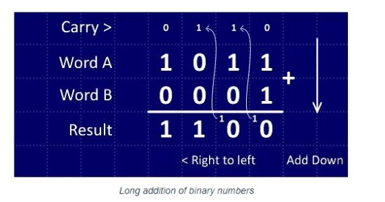
The Circuit
The half adder has two inputs and two outputs as shown in the
diagram below. The two inputs represent two individual bits, the
Sum output represents the sum of the two bits in the form of a
single bit and the Carry output is the carry bit from the
addition.

Binary Subtraction
The Theory
Now that we can add two 4-bit numbers, how do we subtract binary
numbers? To do this, we will implement a binary system called
“two’s complement”. The system has a few rules:
To negate a number (e.g., change 5 into -5), flip all the bits
and add 1.
A number is negative if the MSB (most significant bit) is 1. For
example:
10010 is negative
00010 is positive
Note that by following rule 1 you can determine the value of a
negative binary number:
0001 = 1: Negate this = (1110 + 1 = 1111) = -1
1001 = -7: Negate this = (0110 + 1 = 0111) = 7
0110 = 6: Negate this = (1001 + 1 = 1010) = -6
The two’s complement technique is beneficial because it allows us
to perform both addition and subtraction using the same adder
circuit. So if we wish to turn our 4-bit adder into a 4-bit
adder/subtractor, we just need to incorporate a single 4070 IC
(quad XOR). We feed the binary number inputs into one input of each
XOR gate, use the other XOR input as an add/subtract line, and then
feed this same line into the carry in of the adder.
When we wish to subtract B from A, we make the subtract line high. This does two things:
Flips all the incoming bits on input B
Adds one to the adder

The final circuit will also use a 74HC125 quad buffer on the output so that the adder/subtractor unit can be connected to a common data bus for the output. The buffer also has an enable line that allows us to choose the output from the adder/subtractor.
With the adding/subtracting unit done, it's time to look at the logical functions.
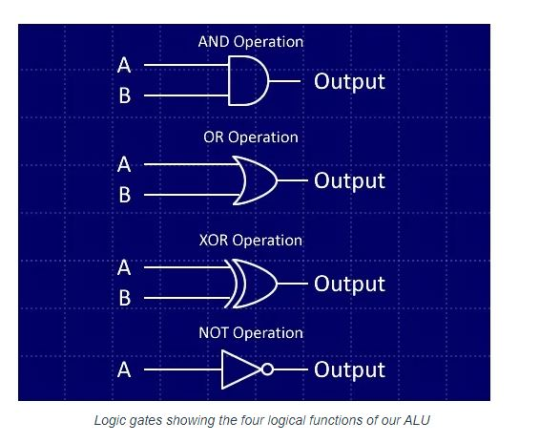
Logical Functions
Logical functions are useful when bit manipulation is needed.
Imagine a microcontroller that has an 8-bit port, and you use the
lower 4 bits to read from a 4-bit data bus. When you read from the
port you will need to remove the upper four bits, as those bits can
affect program execution. So to remove these bits, you can mask
them out with a logical AND function.
This function will AND bits from one word (the port) with another number (the number that will remove the upper four bits). If we AND the port with 0x0F (0b00001111), we preserve the lower four bits (because x AND 1 = x) and remove the upper four bits (because x AND 0 = 0).
AND is used to remove bits
NOT is used when you need to flip all the bits (0000 will become
1111)
OR is used to merge bits (0110 OR 0001 is 0111)
XOR is used to flip selected bits (0101 XOR 0100 is 0001)
The logical units in our ALU are AND, OR, XOR, and NOT gates
connected to buffers. An enable line feeds into each bus buffer for
each logical unit so that each unit can be selected
individually.
4081 - Quad AND gate
4070 - Quad XOR gate
4071 - Quad OR gate
4049 - Hex NOT gate
74HC125 - Output buffers (for bus isolation)
Add Answer to:
Design a 4-bit ALU with the truth table above. In this design A and B are two 4-bit binary inputs, s0, s1, s2, s3 and Ci...
Consider the five-bit binary result (C0, S3, S2, S1, S0) representation in the table above. We...
 Consider the five-bit binary result (C0, S3, S2, S1, S0)
representation in the table above. We would like to represent each
combination as its equivalent in two decimal digits, each of which
can be represented in binary as shown in the following table.
Finish filling in the following truth table. Find the
logic expressions for N2X3, N2X2, N2X1, N2X0, N1X3, N1X2, N1X1, and
N1X0 as a function of C0, S3, S2, S1 and S0 Write the
verilog code for the Binary Coded...
Consider the five-bit binary result (C0, S3, S2, S1, S0)
representation in the table above. We would like to represent each
combination as its equivalent in two decimal digits, each of which
can be represented in binary as shown in the following table.
Finish filling in the following truth table. Find the
logic expressions for N2X3, N2X2, N2X1, N2X0, N1X3, N1X2, N1X1, and
N1X0 as a function of C0, S3, S2, S1 and S0 Write the
verilog code for the Binary Coded...
2d) (10 pts) Design a 2-bit ALU using a 2-bit adder and multiplexors (muxes) for the...
 2d) (10 pts) Design a 2-bit ALU using a 2-bit adder and multiplexors (muxes) for the following operation table W X ALU operation 0 0 A +2 0 1 A & B (bit-wise) 1 0 B >> 1 (filled with 0) A-B Note: To make a connection, instead of drawing a line to make a connection, write a signal at each mux input using al, a, b1, b0, 0, or 1 and/or logic gates if needed. а0 b1 bo si...
Problem 3 - Arithmetie Logic Unit (ALU) Design us poins Design a 4-bit ALU that has two selection...
 Problem 3 - Arithmetie Logic Unit (ALU) Design us poins Design a 4-bit ALU that has two selection variables Si Design an optimized circuit (mus external gates for circuit B operates based on the function table given below. The arithmetic unit and So and generates the arithmetic operations given below. and generatest Use a 4-1 MUX block with Si So Cin = 1 F-A (complement) F = A+B (add) FB (transfer) F A+B F = A+ 1 (negate) F A+B+...
multiple choices Question #4 • Determine the operation performed by the ALU for the given value...
 multiple choices
Question #4 • Determine the operation performed by the ALU for the given value of the select bits. S4 S3 S2 S1 SO = 10 110 OR 4-10-1 Mu MSB LSB TI S3 S2 NOT NAND Addition Subtractio 2-10-1 Mux S1 4-bit Addor Sum Cin Question #5 • Identify the static-1 hazard in the logic circuit given below. XX 0-4 4-5 5-7 0-1 None of the above. FIA,B,C) AB c 0001 11 10 Question #6 • Identify the...
multiple choices
Question #4 • Determine the operation performed by the ALU for the given value of the select bits. S4 S3 S2 S1 SO = 10 110 OR 4-10-1 Mu MSB LSB TI S3 S2 NOT NAND Addition Subtractio 2-10-1 Mux S1 4-bit Addor Sum Cin Question #5 • Identify the static-1 hazard in the logic circuit given below. XX 0-4 4-5 5-7 0-1 None of the above. FIA,B,C) AB c 0001 11 10 Question #6 • Identify the...
5) Decoders: Given the following circuit, S0 and S1 are computed using a 4-2 priority encoder with the priorities indicated on the figure. (hint: IDLE signal is always 0, if any of the inputs...
 5) Decoders: Given the following circuit, S0 and S1 are computed using a 4-2 priority encoder with the priorities indicated on the figure. (hint: IDLE signal is always 0, if any of the inputs 10,11,12, or 13 is 1) 6 points) 4-to-2 Priority Encoder 10 YO YI 13 IDLE 13> 11 > 12>10 12 Full c Adder So Fill the following table showing the output signals S0 and SI given the input signals w, x, y, a) and z. Prof...
WITHOUT using VHDL coding, Design the arithmetic unit by showing the truth tables, expressions and the...
 WITHOUT using VHDL coding, Design the arithmetic unit by
showing the truth tables, expressions and the logic circuits!
How would I also implement the status flags (Z,C,V) in my
circuit?
S2 0 1 1. Design a 4-bit Arithmetic Logic Unit (ALU) according to the following specification. Follow the design shown during the lecture. Notice this table is different, though. A(0:3) B(0:3) S1 So Function (F) 0 0 A+B 0 0 A-B Z ALU 0 0 A-1 0 A +1 0...
WITHOUT using VHDL coding, Design the arithmetic unit by
showing the truth tables, expressions and the logic circuits!
How would I also implement the status flags (Z,C,V) in my
circuit?
S2 0 1 1. Design a 4-bit Arithmetic Logic Unit (ALU) according to the following specification. Follow the design shown during the lecture. Notice this table is different, though. A(0:3) B(0:3) S1 So Function (F) 0 0 A+B 0 0 A-B Z ALU 0 0 A-1 0 A +1 0...
Design a 2-bit alu that performs the following four operations: (However, the internal circuit of the...
Design a 2-bit alu that performs the following four operations: (However, the internal circuit of the full adder may be omitted) s0 s1 operation comment 0 0 clear F=00 0 1 A plus B F=A+B 1 0 A minus B F=A-B 1 1 A exclusive-or B F=A exclusive-or B
FIRST ACTIVITY: (100/100) . SIMPLE 4-BIT ARITHMETIC LOGIC UNIT (ALU): This circuit selects between arithmetic (absolute...
 FIRST ACTIVITY: (100/100) . SIMPLE 4-BIT ARITHMETIC LOGIC UNIT (ALU): This circuit selects between arithmetic (absolute value, addition) and logical (XOR, AND) operations. Only one result (hexadecimal value) can be shown on the 7-segment display This is selected by the input sel (1..0) B A-BI A+B A xnor B A nand B Input EN: If EN-1result appears on the 7 segment display. If EN=0 → all LEDs in the 7 segment display are off Arithmetic operations: The 4-bit inputs A...
You need to design a circuit that implements the functions in the following table: S0 and...
 You need to design a circuit that implements the functions in
the following table:
S0 and S1 are 1-bit control inputs to select the function of the
circuit. Inputs A and B are 4-bit numbers in 2s complement form.
The output is also a 4-bit number in 2s complement form. You are
allowed to use only one TTL 7483 4-bit adder to implement all the
functions. But any number of other components (except the adder)
can be used.
HINT: Design...
You need to design a circuit that implements the functions in
the following table:
S0 and S1 are 1-bit control inputs to select the function of the
circuit. Inputs A and B are 4-bit numbers in 2s complement form.
The output is also a 4-bit number in 2s complement form. You are
allowed to use only one TTL 7483 4-bit adder to implement all the
functions. But any number of other components (except the adder)
can be used.
HINT: Design...
number 4 and 5 please! PROBLEM STATEMENT A logic circuit is needed to add multi-bit binary...
 number 4 and 5 please!
PROBLEM STATEMENT A logic circuit is needed to add multi-bit binary numbers. A 2-level circuit that would add two four-bit numbers would have 9 inputs and five outputs. Although a 2-level SOP or POS circuit theoretically would be very fast, it has numerous drawbacks that make it impractical. The design would be very complex in terms of the number of logic gates. The number of inputs for each gate would challenge target technologies. Testing would...
number 4 and 5 please!
PROBLEM STATEMENT A logic circuit is needed to add multi-bit binary numbers. A 2-level circuit that would add two four-bit numbers would have 9 inputs and five outputs. Although a 2-level SOP or POS circuit theoretically would be very fast, it has numerous drawbacks that make it impractical. The design would be very complex in terms of the number of logic gates. The number of inputs for each gate would challenge target technologies. Testing would...
 Consider the five-bit binary result (C0, S3, S2, S1, S0)
representation in the table above. We would like to represent each
combination as its equivalent in two decimal digits, each of which
can be represented in binary as shown in the following table.
Finish filling in the following truth table. Find the
logic expressions for N2X3, N2X2, N2X1, N2X0, N1X3, N1X2, N1X1, and
N1X0 as a function of C0, S3, S2, S1 and S0 Write the
verilog code for the Binary Coded...
Consider the five-bit binary result (C0, S3, S2, S1, S0)
representation in the table above. We would like to represent each
combination as its equivalent in two decimal digits, each of which
can be represented in binary as shown in the following table.
Finish filling in the following truth table. Find the
logic expressions for N2X3, N2X2, N2X1, N2X0, N1X3, N1X2, N1X1, and
N1X0 as a function of C0, S3, S2, S1 and S0 Write the
verilog code for the Binary Coded...
 2d) (10 pts) Design a 2-bit ALU using a 2-bit adder and multiplexors (muxes) for the following operation table W X ALU operation 0 0 A +2 0 1 A & B (bit-wise) 1 0 B >> 1 (filled with 0) A-B Note: To make a connection, instead of drawing a line to make a connection, write a signal at each mux input using al, a, b1, b0, 0, or 1 and/or logic gates if needed. а0 b1 bo si...
 Problem 3 - Arithmetie Logic Unit (ALU) Design us poins Design a 4-bit ALU that has two selection variables Si Design an optimized circuit (mus external gates for circuit B operates based on the function table given below. The arithmetic unit and So and generates the arithmetic operations given below. and generatest Use a 4-1 MUX block with Si So Cin = 1 F-A (complement) F = A+B (add) FB (transfer) F A+B F = A+ 1 (negate) F A+B+...
 multiple choices
Question #4 • Determine the operation performed by the ALU for the given value of the select bits. S4 S3 S2 S1 SO = 10 110 OR 4-10-1 Mu MSB LSB TI S3 S2 NOT NAND Addition Subtractio 2-10-1 Mux S1 4-bit Addor Sum Cin Question #5 • Identify the static-1 hazard in the logic circuit given below. XX 0-4 4-5 5-7 0-1 None of the above. FIA,B,C) AB c 0001 11 10 Question #6 • Identify the...
multiple choices
Question #4 • Determine the operation performed by the ALU for the given value of the select bits. S4 S3 S2 S1 SO = 10 110 OR 4-10-1 Mu MSB LSB TI S3 S2 NOT NAND Addition Subtractio 2-10-1 Mux S1 4-bit Addor Sum Cin Question #5 • Identify the static-1 hazard in the logic circuit given below. XX 0-4 4-5 5-7 0-1 None of the above. FIA,B,C) AB c 0001 11 10 Question #6 • Identify the...
 5) Decoders: Given the following circuit, S0 and S1 are computed using a 4-2 priority encoder with the priorities indicated on the figure. (hint: IDLE signal is always 0, if any of the inputs 10,11,12, or 13 is 1) 6 points) 4-to-2 Priority Encoder 10 YO YI 13 IDLE 13> 11 > 12>10 12 Full c Adder So Fill the following table showing the output signals S0 and SI given the input signals w, x, y, a) and z. Prof...
 WITHOUT using VHDL coding, Design the arithmetic unit by
showing the truth tables, expressions and the logic circuits!
How would I also implement the status flags (Z,C,V) in my
circuit?
S2 0 1 1. Design a 4-bit Arithmetic Logic Unit (ALU) according to the following specification. Follow the design shown during the lecture. Notice this table is different, though. A(0:3) B(0:3) S1 So Function (F) 0 0 A+B 0 0 A-B Z ALU 0 0 A-1 0 A +1 0...
WITHOUT using VHDL coding, Design the arithmetic unit by
showing the truth tables, expressions and the logic circuits!
How would I also implement the status flags (Z,C,V) in my
circuit?
S2 0 1 1. Design a 4-bit Arithmetic Logic Unit (ALU) according to the following specification. Follow the design shown during the lecture. Notice this table is different, though. A(0:3) B(0:3) S1 So Function (F) 0 0 A+B 0 0 A-B Z ALU 0 0 A-1 0 A +1 0...
 FIRST ACTIVITY: (100/100) . SIMPLE 4-BIT ARITHMETIC LOGIC UNIT (ALU): This circuit selects between arithmetic (absolute value, addition) and logical (XOR, AND) operations. Only one result (hexadecimal value) can be shown on the 7-segment display This is selected by the input sel (1..0) B A-BI A+B A xnor B A nand B Input EN: If EN-1result appears on the 7 segment display. If EN=0 → all LEDs in the 7 segment display are off Arithmetic operations: The 4-bit inputs A...
 You need to design a circuit that implements the functions in
the following table:
S0 and S1 are 1-bit control inputs to select the function of the
circuit. Inputs A and B are 4-bit numbers in 2s complement form.
The output is also a 4-bit number in 2s complement form. You are
allowed to use only one TTL 7483 4-bit adder to implement all the
functions. But any number of other components (except the adder)
can be used.
HINT: Design...
You need to design a circuit that implements the functions in
the following table:
S0 and S1 are 1-bit control inputs to select the function of the
circuit. Inputs A and B are 4-bit numbers in 2s complement form.
The output is also a 4-bit number in 2s complement form. You are
allowed to use only one TTL 7483 4-bit adder to implement all the
functions. But any number of other components (except the adder)
can be used.
HINT: Design...
 number 4 and 5 please!
PROBLEM STATEMENT A logic circuit is needed to add multi-bit binary numbers. A 2-level circuit that would add two four-bit numbers would have 9 inputs and five outputs. Although a 2-level SOP or POS circuit theoretically would be very fast, it has numerous drawbacks that make it impractical. The design would be very complex in terms of the number of logic gates. The number of inputs for each gate would challenge target technologies. Testing would...
number 4 and 5 please!
PROBLEM STATEMENT A logic circuit is needed to add multi-bit binary numbers. A 2-level circuit that would add two four-bit numbers would have 9 inputs and five outputs. Although a 2-level SOP or POS circuit theoretically would be very fast, it has numerous drawbacks that make it impractical. The design would be very complex in terms of the number of logic gates. The number of inputs for each gate would challenge target technologies. Testing would...
Most questions answered within 3 hours.
-
What is the hydroxide ion concentration, [OH-], in a solution
with a hydronium ion concentration, [H3O+]...
asked 6 minutes ago -
For Bergson the concept of Being contains less reality than does
the concept of Becoming. True...
asked 20 minutes ago -
What species is the reducing agent in the following
equation?
Mg(s) + 2HCl (aq) --> MgCl2(aq)...
asked 21 minutes ago -
A 50g ice cube is taken out of a freezer at 0 degrees Celsius
and put...
asked 2 hours ago -
How do ratios help you determine trends? What specific
information do managers look at? Is there...
asked 2 hours ago -
A wavelength of 514 nm is used to find an unknown diffraction
grating. If the separation...
asked 2 hours ago -
Use the central limit theorem to find the mean and standard
error of the mean of...
asked 2 hours ago -
You will be given a file that will contain averages for classes
which are divided into...
asked 2 hours ago -
A Pew Research Center poll surveyed a random sample 850 voters
and asked them if they...
asked 2 hours ago -
Design a class named
NumDays, to
store a value that represents a number of hours and...
asked 2 hours ago -
(R)-2-chloro-(S)-3-bromobutane and
(S)-2-chloro-(S)-3-bromobutane are: A. enantiomers. B.
diastereomers. C. meso compounds. D. the same molecule.
asked 2 hours ago -
1_ What is the Frank-Starling law of the heart? And why the
heart cannot function on...
asked 2 hours ago